
Breakthrough Microscope Makes Hidden 2D Material Visible
Why Study 2D Materials?
Two-dimensional (2D) materials are crystalline substances made of a single layer of atoms. Their extreme thinness gives rise to unusual and often powerful physical properties that do not appear in bulk materials. Although layered materials have been known for over a century, the field truly began in 2004 with the first successful isolation of graphene—a one-atom-thick sheet of carbon.
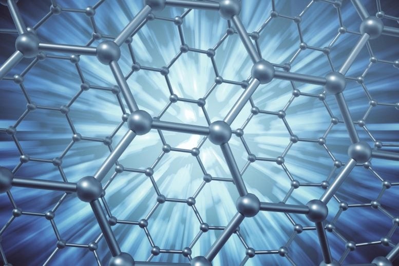
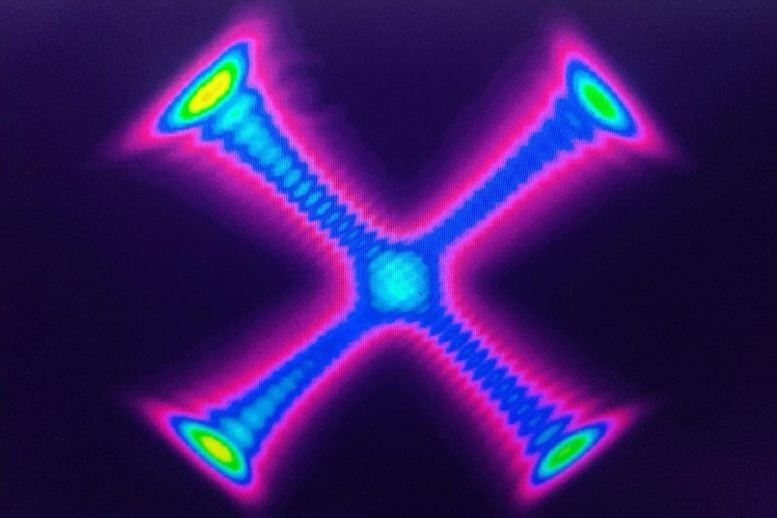
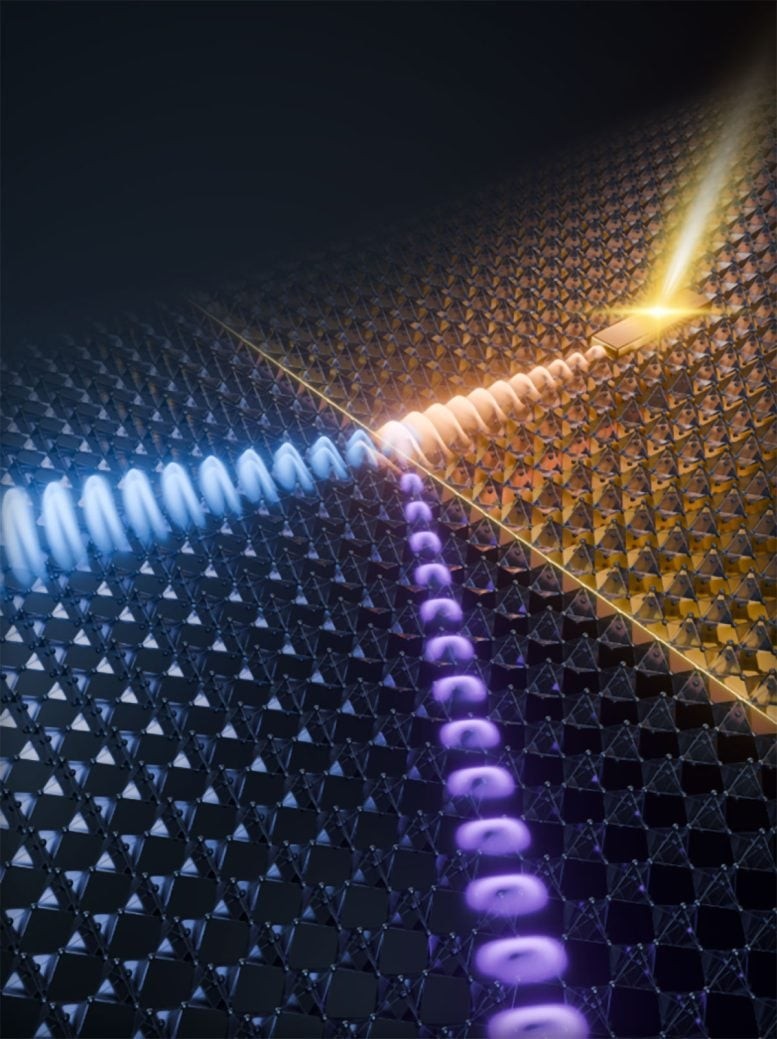
Figure 1. New Microscope Reveals an Invisible 2D Material.
Since then, scientists have discovered and engineered many other 2D materials, revealing a wide range of potential applications. Because these atom-thin layers show promise for next-generation electronics, energy technologies, and optical devices, they remain a major focus of modern materials science. Figure 1 shows New Microscope Reveals an Invisible 2D Material.
The Challenge of Hexagonal Boron Nitride
Boron nitride (BN), often called “white graphene,” is a layered material made of boron and nitrogen atoms. One of its most important forms is hexagonal boron nitride (hBN), which shares graphene’s hexagonal lattice structure. In its 2D form, hBN is widely used in areas such as quantum optics and infrared nanophotonics, and is also commonly employed as a substrate or protective encapsulation layer for other 2D materials.
For these applications, precise characterization of hBN layers is essential. However, aside from a strong resonance in the mid-infrared, monolayer hBN is transparent across the entire near-infrared and visible spectrum. As a result, it cannot be examined using conventional optical microscopes.
This limitation has so far hindered its broader use in the development of advanced materials. For instance, identifying distortions or grain boundaries in 2D layers requires accurate, high-resolution mapping—something standard imaging techniques cannot provide for hBN.
In addition, researchers often stack individual 2D monolayers to form so-called van der Waals structures, which can exhibit entirely new and unexpected properties. Ideally, this stacking process could be monitored in real time under a microscope, with the orientation of each layer clearly visualized. Achieving such capabilities for hBN has therefore been a long-standing goal.
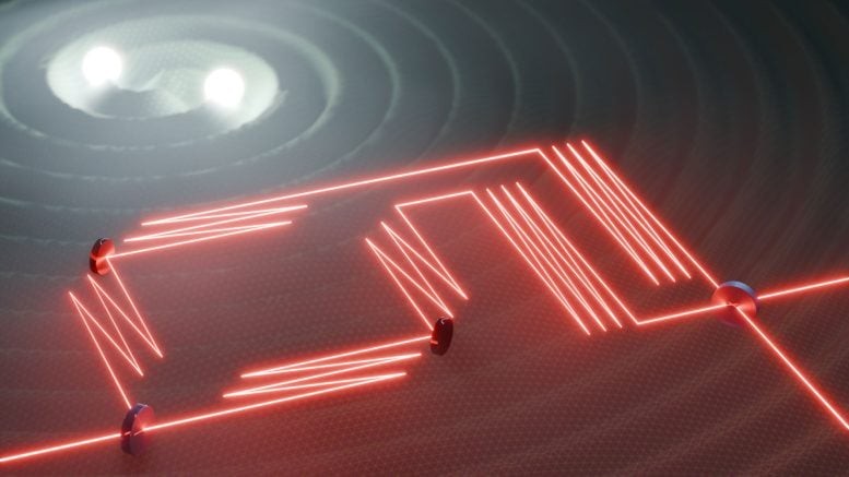
The Sum-Frequency Microscope
A research team at the Fritz Haber Institute has now overcome this challenge by developing a new microscope that uses a nonlinear-optics technique to make otherwise invisible hBN visible. Their approach, known as phase-resolved sum-frequency microscopy, combines two laser beams—one in the mid-infrared and one in the visible range—to generate a measurable sum-frequency signal within the sample.
By resonantly exciting a lattice vibration in hBN, this signal becomes exceptionally strong. This allows researchers to image large areas (up to 100 × 100 μm²) in under one second and even directly visualize the crystal orientation of the material.By resonantly exciting a lattice vibration in hBN, this signal becomes exceptionally strong. This allows researchers to image large areas (up to 100 × 100 μm²) in under one second and even directly visualize the crystal orientation of the material.
Using their new microscope, the researchers discovered that hBN monolayers grown in triangular domains feature nitrogen-terminated zigzag edges. In addition, the strong nonlinear response observed near the vibrational resonance identifies monolayer hBN as a highly promising material for frequency upconversion—from the infrared into the visible—in next-generation optoelectronic devices.
Prospects of the New Experimental Method
The newly developed microscope offers several key advantages over existing techniques. Most notably, it enables optically transparent materials to be visualized using an optical microscope. The resulting images provide significantly higher contrast than conventional AFM images, while vibrational-resonance enhancement allows for live imaging of hBN, including real-time information about crystal orientation.
Together, these capabilities pave the way for controlled fabrication of layered van der Waals structures in future applications. Beyond hBN, the authors anticipate that this imaging approach can be extended as a non-invasive, label-free technique for studying a wide range of stacked 2D materials, as well as their integration with anisotropic molecular assemblies.
Source:SciTECHDaily
Cite this article:
Priyadharshini S (2025), Breakthrough Microscope Makes Hidden 2D Material Visible, AnaTechMaz, pp. 332
Recent Post
-
High-Energy Vortex Lasers Poised to Revolutionize Manufacturing and Imaging
Optical vortices—light beams carrying orbital angular momentum—...
-
Breakthrough Microscope Makes Hidden 2D Material Visible
Two-dimensional (2D) materials are crystalline substances made of a single layer of atoms. Their extreme...
-
Eco-Friendly Scientific Breakthrough Promises to Eliminate “Forever Chemicals”
PFAS, or per- and polyfluoroalkyl substances, are a large group of...
-
Physicists Outline the First Experimental Plan to Control Gravitational Waves
“Gravity influences everything, including light,” explains Schützhold. When...
-

Researchers Uncover Hidden Battery Flaw Behind Short Lifespan and Fire Hazards
“Until now, attempts to transition to single-crystal cathodes largely,...
-
Scientists Break Records by Precisely Steering Light at the Nanoscale
To overcome this challenge, researchers from Shanghai Jiao ,....
-
MIT Engineers Develop 3D-Printable Aluminum Five Times Stronger Than Standard Alloys
As a challenge, Olson asked the class to create an aluminum alloy...