
Introducing MEGA2D: The Compact Machine Revolutionizing the Future of Material Science
A groundbreaking device allows scientists to effortlessly fine-tune the twist between layers of ultra-thin materials, paving the way for major breakthroughs in electronics and optics. This innovation could improve transistors and solar cells while advancing quantum computing research.
Six years ago, a groundbreaking discovery reshaped condensed-matter physics: ultra-thin carbon layers stacked at slight angles were found to become superconductors. Researchers revealed that adjusting the twist angle between these layers allowed precise control over the material’s electrical properties. This discovery, featured in a landmark 2018 paper on “magic-angle graphene superlattices,” sparked the emergence of a new field called “twistronics.” Yuan Cao, then an MIT graduate student and later a Harvard Junior Fellow, was the paper’s lead author.

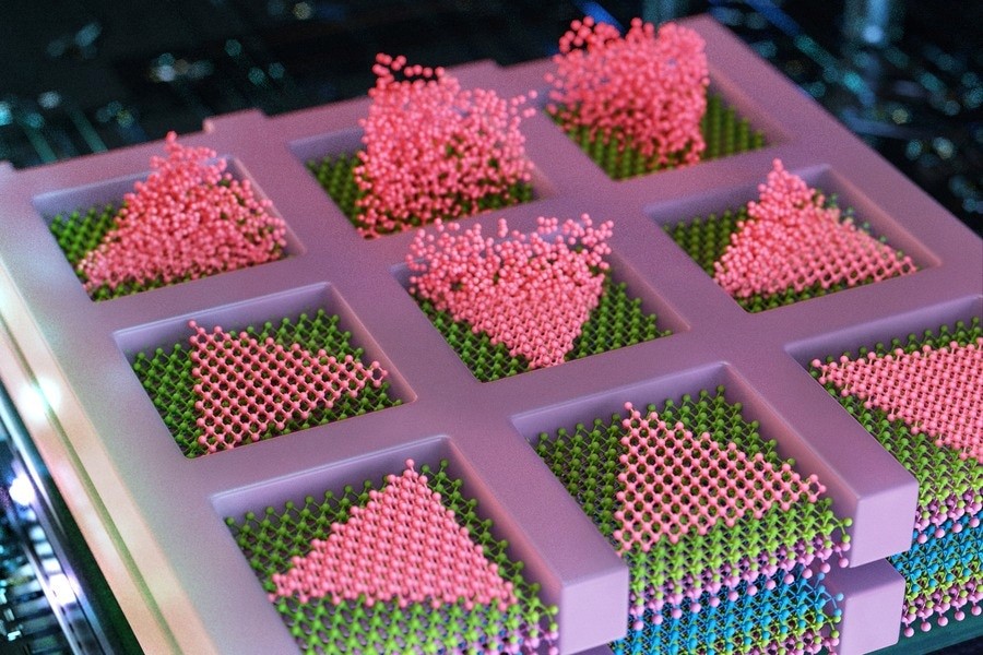
Figure 1. Tiny Machine Manipulates Angles in Layered Materials for Breakthroughs in Tech and Material Science
Building on this transformative work, Cao, alongside Harvard physicists Amir Yacoby, Eric Mazur, and their team, has developed a more efficient technique to manipulate and study a broader range of materials, driving further progress in the field of twistronics [1]. Figure 1 shows Tiny Machine Manipulates Angles in Layered Materials for Breakthroughs in Tech and Material Science.
Unveiling MEGA2D: A Revolutionary Tool for Material Manipulation
A recent paper in Nature introduces the team’s innovative fingernail-sized device, capable of twisting thin materials on demand, eliminating the need to fabricate twisted devices individually. These ultra-thin 2D materials, which can now be easily studied and manipulated, hold immense potential for advancing high-performance transistors, solar cells, quantum computers, and more.
“This breakthrough makes twisting as straightforward as controlling the electron density of 2D materials,” said Amir Yacoby, Harvard professor of physics and applied physics. “Electron density has been the key parameter for uncovering new phases of matter in low-dimensional systems. Now, with the ability to control both density and twist angle, the possibilities for discovery are limitless.”
Challenges and Innovations in Creating Twisted Devices
As a graduate student in Pablo Jarillo-Herrero’s lab at MIT, Yuan Cao first created twisted bilayer graphene, a groundbreaking achievement tempered by the challenge of replicating the precise twisting process.
“At the time, each twisted device was difficult to produce, making the process both unique and time-consuming,” Cao explained. To advance their research, they needed tens or even hundreds of these devices. This led to the idea of creating “one device to twist them all,” Cao said—a micromachine capable of twisting two layers of material on demand, eliminating the need for countless individual samples. The result is MEGA2D, a MEMS (micro-electromechanical system)-based generic actuation platform for 2D materials.
Future Prospects and Applications of Twistronics
The Yacoby and Mazur labs joined forces to design this versatile tool kit, which can be applied to graphene and other materials.
“With this new ‘knob’ provided by our MEGA2D technology, we believe many fundamental challenges in twisted graphene and other materials could be easily resolved,” said Yuan Cao, now an assistant professor at the University of California, Berkeley. “It will undoubtedly lead to new discoveries along the way.”
In their paper, the researchers showcased the device’s capabilities using two pieces of hexagonal boron nitride, a close relative of graphene. They successfully explored the bilayer device’s optical properties, uncovering evidence of quasiparticles with desirable topological characteristics.
The simplicity of their new system opens up numerous scientific possibilities, such as using hexagonal boron nitride twistronics to create light sources for low-loss optical communication.
“We hope our approach will be embraced by many other researchers in this rapidly advancing field, allowing everyone to benefit from these new capabilities,” Cao said.
Turning Concept into Reality: The Development of MEGA2D
The paper’s first author, Haoning Tang, a nanoscience and optics expert, postdoctoral researcher in Mazur’s lab, and Harvard Quantum Initiative fellow, emphasized that developing the MEGA2D technology was a lengthy process of trial and error.
“We didn’t know much about how to control the interfaces of 2D materials in real time, and the existing methods just weren’t effective,” she explained [2]. “After spending countless hours in the cleanroom and refining the MEMS design—despite many failed attempts—we finally found a successful solution after about a year of experiments.” All nanofabrication was carried out at Harvard’s Center for Nanoscale Systems, where the staff provided essential technical support, Tang added.
Impacts on Optics and Photonics
“The nanofabrication of a device that integrates MEMS technology with a bilayer structure is a true tour de force,” said Mazur, the Balkanski Professor of Physics and Applied Physics. “The ability to tune the nonlinear response of the resulting device unlocks a whole new category of possibilities in optics and photonics.”
References:
- https://engineering.berkeley.edu/news/2024/08/worlds-first-micromachine-twists-2d-materials-at-will/
- https://scitechdaily.com/meet-mega2d-the-tiny-machine-twisting-material-science-into-the-future/
Cite this article:
Janani R (2025), Introducing MEGA2D: The Compact Machine Revolutionizing the Future of Material Science, AnaTechMaz, pp. 90
Recent Post
-
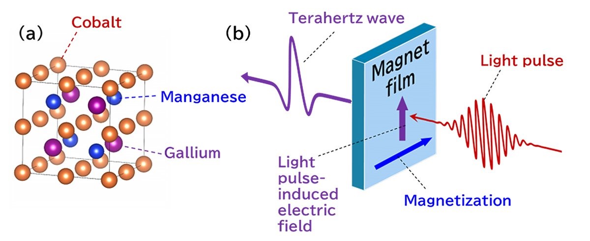
New Magnetic Material Could Revolutionize Terahertz Wave Technology for Future Applications
Terahertz waves are attracting increasing attention from researchers worldwide...
-

Engineers Make CO2 Conversion into Useful Products More Practical
New Electrode Design Enhances CO2 Conversion Efficiency into Useful Products...
-
Quantum Material Senses Minute Mechanical Strains
A new sensor developed at Nanjing University, China, can detect...
-

Magnetic "Metasheet" Material Can Move Objects Like a Conveyor Belt
Scientists at North Carolina State University (NCSU) have developed a...
-
A Reaction Inspired by Rocket Technology Produces Carbon with An Unprecedented Surface Area
Researchers have applied principles from rocket science to create...
-

Glow-In-The-Dark Wood Provides Passive Lighting for Homes or Parks
Picture a glow-in-the-dark designer desk or wooden fence posts lighting the...
-

2D Materials with a 'Twist' Reveal Unexpected Electronic Properties
In the quest for new materials to enable more efficient electronics, scientists...
-
Major Players in Nuclear Fusion and Quantum Tech in 2024
Each passing year brings us closer to groundbreaking advancements in...
-
Airframe Designs Pioneers a Blended Approach to Tooling Design
With the growing adoption of additive manufacturing, our blended...
-
High-Speed Interconnections for Scalable 3D Chip Design
The electronics industry is nearing the limits of transistor integration on a single ...
-

Atomic Spray Painting Revolutionizes Material Science for More Sustainable Technology
Scientists can precisely adjust a material's properties for advanced applications...
-

Scientists Achieve the Impossible by Manipulating Molecules with Light
A research team led by Prof. Alberto Credi at the University of Bologna...
-
Japanese Scientists Reveal Revolutionary 3D Printing Breakthrough for Lightweight Cars
Metal 3D printing involves constructing objects layer by layer, bonding metal layers...
-
Princeton Scientists Create Innovative New Material: Stretchable, Flexible, And Recyclable
The material's exceptional performance is rooted in its internal structure at the ...
-
Introducing MEGA2D: The Compact Machine Revolutionizing the Future of Material Science
A groundbreaking device allows scientists to effortlessly fine-tune the...