
Atomic Spray Painting Revolutionizes Material Science for More Sustainable Technology
Scientists can precisely adjust a material's properties for advanced applications by manipulating its atomic structure. A team led by researchers at Penn State has found that "atomic spray painting" of potassium niobate—a crucial material for advanced electronics—offers exceptional control over thin-film properties. Their study, published in Advanced Materials, could lead to more sustainable technologies in consumer electronics, medical devices, and quantum computing.
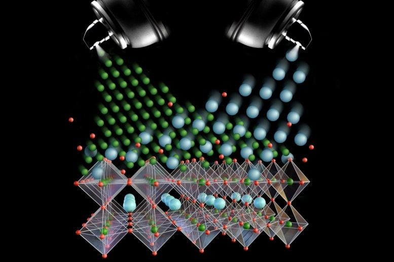
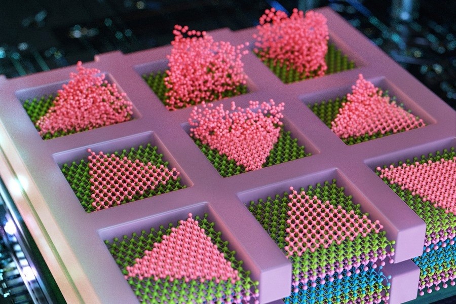
Figure 1. Atomic Spray Painting Transforms Material Science for Sustainable Technology Advancements.
The technique, called strain tuning, alters a material's properties by stretching or compressing its atomic unit cell, which is the repeating pattern of atoms in its crystal structure. The team utilized molecular beam epitaxy (MBE), a method for depositing atomic layers onto a substrate to create thin films. This approach enabled them to produce a strain-tuned thin film of potassium niobate with remarkable precision. Figure 1 shows Atomic Spray Painting Transforms Material Science for Sustainable Technology Advancements.
"This is the first time potassium niobate has been grown using MBE," said Venkatraman "Venkat" Gopalan, a professor of materials science and engineering at Penn State and corresponding author of the study. "The technique is like spray-painting atoms onto a surface."
This method enables the atoms in thin films to adapt to the atomic structure of the underlying substrate, creating strain, explained co-author Sankalpa Hazra, a doctoral candidate in materials science and engineering. "Even a small stretch of about 1% can create pressure that would be impossible to achieve by simply pulling or pressing on such a brittle material from the outside. This pressure significantly enhances the material’s ferroelectric performance."
Ferroelectric Properties and Applications
Potassium niobate is a ferroelectric material, meaning it has a natural electric polarization that can be reversed by applying an external electric field—similar to how magnets can flip their magnetic polarity.
“A ferroelectric is like a mini battery that is permanently charged by nature,” said Gopalan. “Though not widely known, ferroelectrics are essential to key technologies in everyday life. For instance, the internet relies on ferroelectric crystals to convert electrical signals into optical signals. These materials are also crucial for devices like ultrasound equipment, infrared cameras, and precision actuators used in advanced microdevices.”
Collaborative Research and Development
To achieve the "atomic spray painting" of potassium niobate, Gopalan collaborated with Darrell Schlom, a former Penn State colleague who now works at Cornell University. The team grew the thin films at the U.S. National Science Foundation-funded Platform for the Accelerated Realization, Analysis, and Discovery of Interface Materials (PARADIM) facility, which Schlom co-directs at Cornell. Schlom highlighted that he and Gopalan had previously worked together on the first strain-tuning of ferroelectric materials nearly 20 years ago.
“Our role was to help Venkat and Sankalpa realize this material that Venkat has been envisioning for decades,” said Schlom. “Venkat had synthesized unstrained thin films of this material during his doctoral research at Cornell three decades ago, so he knows how challenging it can be to grow it. My student, Tobias Schwaigert, and I assisted them in growing this material.”
Impact of Strain Engineering
Strain engineering works by layering two materials with slightly different atomic sizes. When atoms are deposited onto a surface with a slightly different atomic arrangement, the thin layer adjusts to match, creating strain in the material, similar to how a rubber band stretches. This strain leads to changes in the material's properties, enhancing its temperature tolerance and ferroelectric performance.
“The exceptional coupling between strain and polarization in potassium niobate compared to other ferroelectrics allows for significant changes in both the material’s ferroelectric structure and its polarization with relatively small amounts of strain,” Hazra said. “This superior strain sensitivity enables the ferroelectric performance of potassium niobate to surpass that of lead titanate and lead zirconate titanate, which are the industrial standards for ferroelectric applications.”
Environmental and Practical Implications
This discovery is especially important because potassium niobate is lead-free. Lead, while common in ferroelectric materials like lead titanate and lead zirconate titanate, raises concerns due to its toxicity. Without strain tuning, potassium niobate's ferroelectric properties are weaker than those of lead-based materials, but this study demonstrates its potential as a safer, environmentally friendly alternative.
The research team also found that strain-tuned potassium niobate maintains its ferroelectric properties even at high temperatures. Generally, ferroelectric materials lose their polarization when heated, rendering them incapable of switching electrical charges.
“In our work, we’ve shown that applying strain increases the temperature at which the material loses its ferroelectric properties,” said Gopalan. “With just 1% strain, we can raise the temperature threshold to over 975 degrees Kelvin, just below the point where the material starts to degrade.”
Future Directions and Applications
The next challenge for the researchers is growing these thin films on silicon, which is widely used in electronics. Gopalan’s team is also working on fine-tuning the film growth process to improve the electrical properties of the material, paving the way for practical applications. Strain-tuned potassium niobate could be used in advanced devices like high-temperature memory storage for space exploration, quantum computing, and environmentally friendly high-tech applications.
“With further development, this new material could become a key component in the next generation of green, high-performance technologies, impacting everything from personal devices to space exploration,” said Gopalan.
Source:SciTECHDaily
Cite this article:
Priyadharshini S (2024), Atomic Spray Painting Revolutionizes Material Science for More Sustainable Technology, AnaTechMaz, pp. 86
Recent Post
-
New Magnetic Material Could Revolutionize Terahertz Wave Technology for Future Applications
Terahertz waves are attracting increasing attention from researchers worldwide...
-

Engineers Make CO2 Conversion into Useful Products More Practical
New Electrode Design Enhances CO2 Conversion Efficiency into Useful Products...
-
Quantum Material Senses Minute Mechanical Strains
A new sensor developed at Nanjing University, China, can detect...
-
Magnetic "Metasheet" Material Can Move Objects Like a Conveyor Belt
Scientists at North Carolina State University (NCSU) have developed a...
-
A Reaction Inspired by Rocket Technology Produces Carbon with An Unprecedented Surface Area
Researchers have applied principles from rocket science to create...
-
Glow-In-The-Dark Wood Provides Passive Lighting for Homes or Parks
Picture a glow-in-the-dark designer desk or wooden fence posts lighting the...
-

2D Materials with a 'Twist' Reveal Unexpected Electronic Properties
In the quest for new materials to enable more efficient electronics, scientists...
-
Major Players in Nuclear Fusion and Quantum Tech in 2024
Each passing year brings us closer to groundbreaking advancements in...
-
Airframe Designs Pioneers a Blended Approach to Tooling Design
With the growing adoption of additive manufacturing, our blended...
-
High-Speed Interconnections for Scalable 3D Chip Design
The electronics industry is nearing the limits of transistor integration on a single ...
-
Atomic Spray Painting Revolutionizes Material Science for More Sustainable Technology
Scientists can precisely adjust a material's properties for advanced applications...
-

Scientists Achieve the Impossible by Manipulating Molecules with Light
A research team led by Prof. Alberto Credi at the University of Bologna...
-
Japanese Scientists Reveal Revolutionary 3D Printing Breakthrough for Lightweight Cars
Metal 3D printing involves constructing objects layer by layer, bonding metal layers...
-
Princeton Scientists Create Innovative New Material: Stretchable, Flexible, And Recyclable
The material's exceptional performance is rooted in its internal structure at the ...
-

Introducing MEGA2D: The Compact Machine Revolutionizing the Future of Material Science
A groundbreaking device allows scientists to effortlessly fine-tune the...