
High-Speed Interconnections for Scalable 3D Chip Design
The electronics industry is nearing the limits of transistor integration on a single chip surface. To overcome this, manufacturers are shifting focus from further miniaturization to vertical stacking. This approach involves layering multiple surfaces of transistors and semiconducting components, much like transforming a single-story structure into a skyscraper. Such multilayered chips have the potential to perform more complex computations and manage far greater data volumes than current designs.
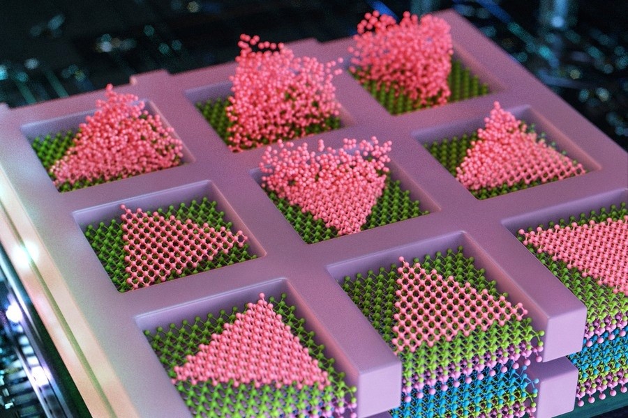
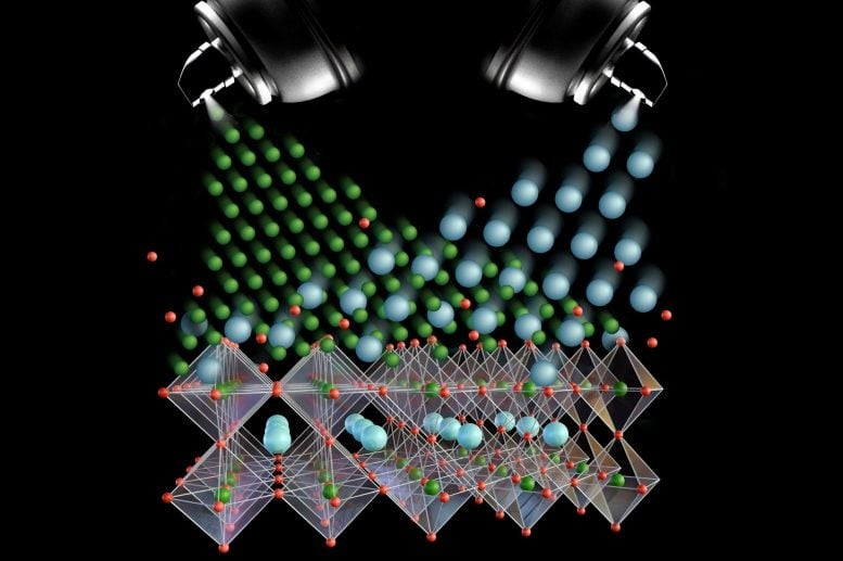
Figure 1. Scalable 3D Chip Design with High-Speed Interconnections
A key challenge with stacking chips lies in the conventional use of silicon wafers as the foundation for semiconductor construction. In standard designs, each layer requires a thick silicon substrate, which hinders communication between the functional layers. Figure 1 shows Scalable 3D Chip Design with High-Speed Interconnections.
MIT engineers have developed a multilayer chip design that eliminates the need for silicon wafer substrates while maintaining low-temperature operation to protect underlying circuitry. This innovative method enables the direct growth of high-performance semiconducting layers atop one another.
Instead of relying on bulky silicon wafers, this approach allows the creation of transistors, memory, and logic components on diverse crystalline surfaces. Removing the thick silicon substrates reduces the distance between semiconducting layers, enhancing interlayer communication and improving computational efficiency.
The researchers propose that this technique could revolutionize AI hardware, enabling stacked chips for devices like laptops and wearables to achieve performance levels akin to modern supercomputers, with data storage capacities rivaling those of data centers.
Atomic Seed Pockets
In 2023, Kim's team introduced a method for cultivating high-quality semiconducting materials on amorphous surfaces, replicating the intricate topography of semiconductor circuitry on completed chips. Their work focused on a category of two-dimensional materials known as transition-metal dichalcogenides (TMDs), which show great potential as an alternative to silicon for creating high-performance, miniaturized transistors. Unlike silicon, which suffers performance loss at atomic scales, these 2D materials maintain their semiconducting properties even at extremely small dimensions.
Previously, the team successfully grew TMDs on both existing TMD layers and silicon wafers with amorphous coatings. This process involved using a thin silicon dioxide "mask" with tiny holes or pockets etched into it. Applied over a silicon wafer, the mask guided the arrangement of atoms into high-quality, single-crystalline structures instead of disordered polycrystalline forms. When exposed to an atom-rich gas, the atoms settled into these pockets, serving as "seeds" that developed into ordered, single-crystalline patterns.
Layered Innovation
Kim and his team focused on refining their method to grow single-crystalline 2D materials at low temperatures, preserving existing transistor circuitry. Drawing inspiration from metallurgy, they noted how molten metal nucleates at mold edges, forming grains that grow into patterned crystals as the metal cools. Metallurgists have observed that edge nucleation requires less energy and heat.
“It’s known that nucleating at the edges requires less energy — and heat. So, we borrowed this concept from metallurgy for future AI hardware,” Kim explained.
The researchers aimed to grow single-crystalline TMDs directly onto silicon wafers embedded with transistor circuitry. Using a silicon dioxide mask similar to their earlier work, they found that TMD seeds placed at the edges of each pocket grew into single-crystalline material at just 380 ℃. In contrast, seeds at the center required higher temperatures to achieve similar results.
Expanding on this approach, the team developed a method to fabricate multilayered chips with alternating layers of two distinct TMDs: tungsten diselenide, ideal for p-type transistors, and molybdenum disulfide, suited for n-type transistors. These transistors are essential components of logic circuits.
By eliminating intermediate silicon wafers, the team successfully grew both materials in single-crystalline form, one directly on top of the other. This advancement could potentially double the density of semiconducting components, particularly CMOS devices, which are vital to modern logic operations.
Kim remarked, “Our technique enables not just 3D logic chips but also 3D memory and their combinations. Using our growth-based monolithic 3D method, you could build tens to hundreds of logic and memory layers directly on top of each other, with excellent interlayer communication.”
He highlighted the limitations of conventional 3D chip fabrication, which relies on silicon wafers with drilled holes for interconnects, restricting the number of layers, vertical alignment precision, and production yields. “Our growth-based method overcomes all these challenges simultaneously,” he added.
To drive the commercialization of their stackable chip technology, Kim founded FS2 (Future Semiconductor 2D materials).
“So far, we’ve demonstrated the concept on small-scale device arrays,” Kim said. “The next step is to scale up and showcase professional AI chip functionality.”
Source:AZO MATERIALS
Cite this article:
Priyadharshini S (2024), High-Speed Interconnections for Scalable 3D Chip Design, AnaTechMaz, pp. 85
Recent Post
-
New Magnetic Material Could Revolutionize Terahertz Wave Technology for Future Applications
Terahertz waves are attracting increasing attention from researchers worldwide...
-

Engineers Make CO2 Conversion into Useful Products More Practical
New Electrode Design Enhances CO2 Conversion Efficiency into Useful Products...
-

Quantum Material Senses Minute Mechanical Strains
A new sensor developed at Nanjing University, China, can detect...
-

Magnetic "Metasheet" Material Can Move Objects Like a Conveyor Belt
Scientists at North Carolina State University (NCSU) have developed a...
-
A Reaction Inspired by Rocket Technology Produces Carbon with An Unprecedented Surface Area
Researchers have applied principles from rocket science to create...
-

Glow-In-The-Dark Wood Provides Passive Lighting for Homes or Parks
Picture a glow-in-the-dark designer desk or wooden fence posts lighting the...
-

2D Materials with a 'Twist' Reveal Unexpected Electronic Properties
In the quest for new materials to enable more efficient electronics, scientists...
-
Major Players in Nuclear Fusion and Quantum Tech in 2024
Each passing year brings us closer to groundbreaking advancements in...
-
Airframe Designs Pioneers a Blended Approach to Tooling Design
With the growing adoption of additive manufacturing, our blended...
-
High-Speed Interconnections for Scalable 3D Chip Design
The electronics industry is nearing the limits of transistor integration on a single ...
-
Atomic Spray Painting Revolutionizes Material Science for More Sustainable Technology
Scientists can precisely adjust a material's properties for advanced applications...
-

Scientists Achieve the Impossible by Manipulating Molecules with Light
A research team led by Prof. Alberto Credi at the University of Bologna...
-
Japanese Scientists Reveal Revolutionary 3D Printing Breakthrough for Lightweight Cars
Metal 3D printing involves constructing objects layer by layer, bonding metal layers...
-
Princeton Scientists Create Innovative New Material: Stretchable, Flexible, And Recyclable
The material's exceptional performance is rooted in its internal structure at the ...
-

Introducing MEGA2D: The Compact Machine Revolutionizing the Future of Material Science
A groundbreaking device allows scientists to effortlessly fine-tune the...