
AI Hardware Breakthrough: Scientists Build Largest-Ever Spin Waveguide Network
Researchers from the Universities of Münster and Heidelberg, led by Prof. Rudolf Bratschitsch, have developed a new method that allows spin waves to travel significantly longer distances through waveguides, paving the way for more energy-efficient AI hardware. As the demand for AI grows, so does the strain on global energy systems—driving the need for innovative computing technologies. Spin waves, which can carry and process information, offer a promising alternative. Using their new technique, the team built the largest spin waveguide network to date and demonstrated precise control over wave properties such as wavelength and boundary reflections. The breakthrough was published in Nature Materials.

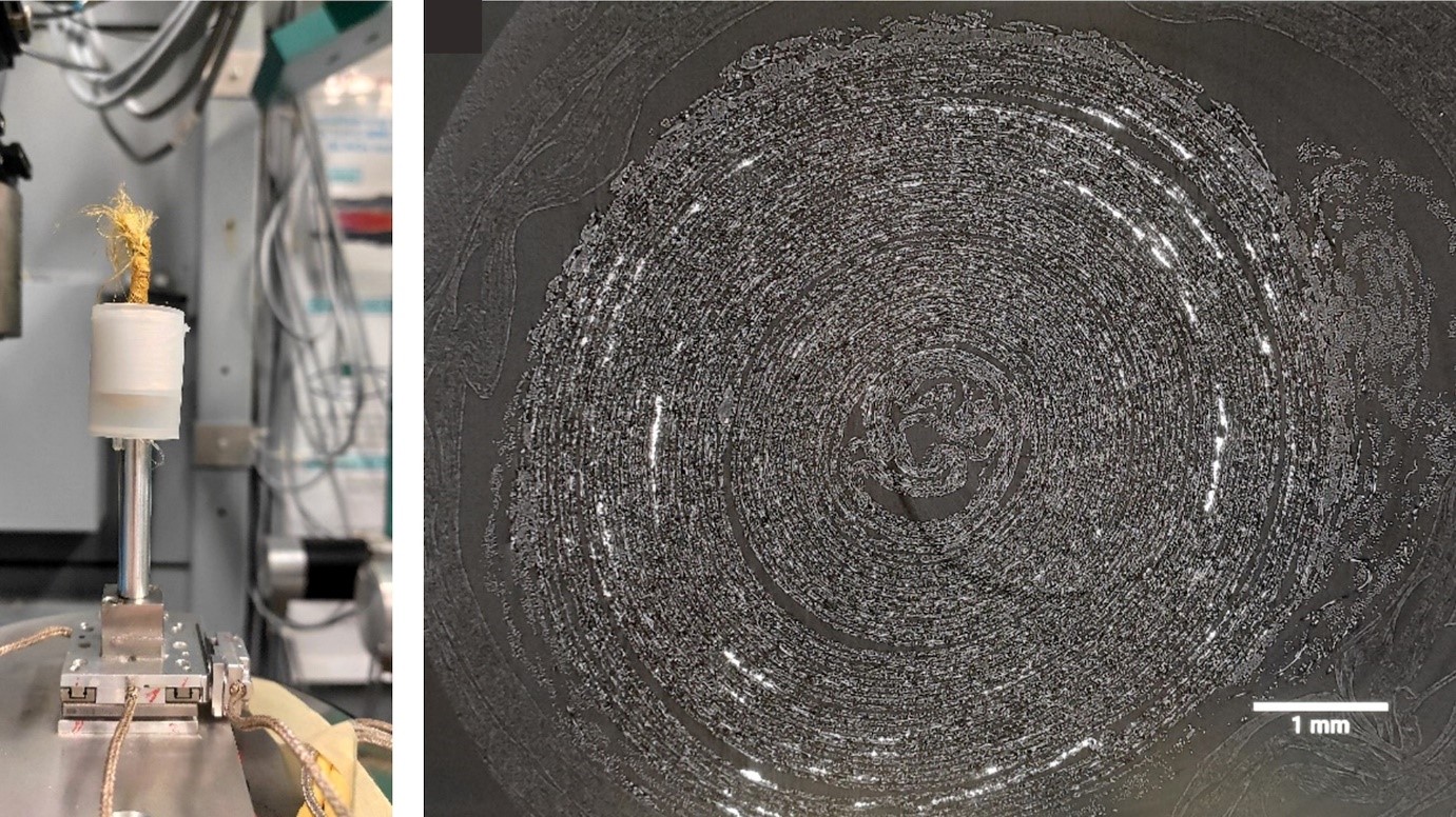
Figure 1. Visualization of a Spin Waveguide Network Created with an Ion Beam (Bottom: Antenna and Network; Top Right: Ion Beam; Top Left: Spin Wave).
Exploring Spin Waves and Their Magnetic Properties
Electron spin, a quantum property representing intrinsic angular momentum, plays a key role in determining a material's magnetic characteristics through the collective alignment of spins. When an alternating current is applied to a magnetic material using an antenna, it produces a varying magnetic field that can excite spin waves within the material. Figure 1 shows Visualization of a Spin Waveguide Network Created with an Ion Beam (Bottom: Antenna and Network; Top Right: Ion Beam; Top Left: Spin Wave).
Spin waves have previously been harnessed to build individual components like logic gates—which convert binary inputs into outputs—and multiplexers that choose among multiple input signals. However, these components had not yet been integrated into a larger, connected circuit—until now.
According to Rudolf Bratschitsch, the challenge in building larger spin-wave networks—similar to those in electronics—has been the significant attenuation of spin waves within nanoscale waveguides, especially those narrower than a micrometer. To overcome this, the research team used yttrium iron garnet (YIG), a material known for having the lowest spin-wave attenuation [1]. They etched individual waveguides into a 110-nanometer-thick YIG film using a silicon ion beam and successfully created a large network consisting of 198 nodes. This new method enables the flexible and reproducible fabrication of complex, high-quality spin-wave structures.
References:
- https://scitechdaily.com/ai-hardware-revolution-scientists-create-largest-spin-waveguide-network/
Cite this article:
Janani R (2025), AI Hardware Breakthrough: Scientists Build Largest-Ever Spin Waveguide Network, AnaTechMaz, pp. 242
Recent Post
-

Researchers Turn Carbon Waste Into High-Value Construction Material
Researchers have developed a low-lead process to convert carbon....
-
AI Hardware Breakthrough: Scientists Build Largest-Ever Spin Waveguide Network
Researchers from the Universities of Münster and Heidelberg, led by....
-

Tiny Structure Defies a Core Principle of Optics
Scientists have overcome a fundamental limitation in optics by using innovative bilayer metagratings...
-

One New Alloy Could Revolutionize Phones, Laptops, and Data Centers
Researchers at the University of Minnesota have introduced a groundbreaking new alloy....
-
X-ray Scans Uncover Buddhist Prayers Hidden Within Tiny Tibetan Scrolls
A delicate antique Buddhist scroll, once part of a traditional Mongolian...
-

AI Unlocks the Future of Batteries — And It’s Not Lithium
Recent discoveries suggest that the future of energy storage may lie in more affordable, safer, and...
-

Salt Additive Solves Hidden Water Problem, Boosts Battery Lifespan by 10x
ater was quietly undermining battery performance—until...
-

New 3D Printing Innovation Paves the Way for Affordable, High-Strength Titanium
Brooke, who was recently awarded a Research Translation Fellowship...
-

quasicrystals: When Matter Plays by Its Own Rules
For decades, quasicrystals—mysterious solids that seem to straddle the line between crystal and...
-

UK to Produce Nuclear Reactor Graphite from Recycled Materials to Reduce Waste
The University of Manchester has secured funding to lead a...
-

Scientists Capture First-Ever Real-Time Look at Electrolytes in Lithium-Sulfur Batteries
For the first time, researchers at Helmholtz-Zentrum Berlin (HZB) ...
-

Slime-Inspired Electrolyte May Improve Lithium-Ion Battery Safety and Recyclability
In a bid to make lithium-ion batteries safer, cleaner, and easier to...
-

New AI Approach Accelerates Calculations to Shield Fusion Reactors from Plasma Heat
A team of US researchers has introduced a groundbreaking...
-
Reinventing Solar: “Black Metal” Device Boosts Power Output 15-Fold
As the world looks for cleaner and more independent energy solutions, researchers have long studied...
-

Flat Band Discovery in Superconductors May Pave the Way for Next-Gen Computing
Kagome metals—materials with distinctive two-dimensional...