

Pixel by Pixel: MIT Redefines Infrared Camera Technology
Researchers at MIT have developed a programmable infrared chip that could transform the future of thermal imaging by replacing bulky moving optics with precise electronic control at the pixel level. Designed as a compact semiconductor-based infrared lens, the technology enables cameras to dynamically manipulate incoming infrared light without mechanical components, paving the way for smaller, smarter, and more versatile imaging systems. The innovation could benefit applications ranging from environmental monitoring and industrial inspection to defense, scientific research, and future optical computing.
Unlike conventional infrared cameras that rely on mechanical lenses or moving parts to adjust focus and capture different types of information, the new device controls light electronically through millions of microscopic pixels. Each pixel can independently modify how it interacts with mid-infrared light, allowing the system to adapt its optical properties in real time. This programmable approach enables a single camera to collect richer and more detailed information from the same scene while remaining compact and energy efficient.
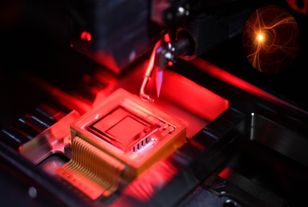
Figure 1. Camera Technology.
The breakthrough is made possible by combining a phase-change material with a crossbar network of copper wires, a design inspired by display technologies. Tiny regions of the phase-change material are switched between crystalline and amorphous states using heat generated through doped silicon, altering the way each pixel manipulates infrared light. Unlike earlier programmable metasurfaces that either controlled an entire lens at once or required complex wiring for every individual pixel, the crossbar architecture enables scalable two-dimensional pixel control while minimizing electrical interference. This design could eventually support devices with millions of programmable pixels using semiconductor manufacturing techniques already common in the electronics industry.
To validate the concept, the research team fabricated a 6 × 6 metasurface pixel array and demonstrated that it could repeatedly switch between optical states without losing performance. The successful prototype shows that programmable infrared optics can be integrated into semiconductor chips, opening the possibility of large-scale manufacturing for future imaging devices. Figure 1 shows camera technology.
The technology has significant potential across multiple fields. Because many gases and organic molecules strongly absorb mid-infrared light, the chip could enhance systems used for detecting methane, propane, and other atmospheric compounds, improving environmental monitoring and industrial safety [1]. It could also lead to more advanced thermal imaging cameras for medical diagnostics, scientific exploration, autonomous systems, and night-vision equipment. Beyond imaging, the researchers believe programmable metasurfaces could contribute to optical computing, where light performs computational tasks more efficiently than conventional electronic circuits.
Looking ahead, the MIT team plans to increase the number of programmable pixels and further improve the durability of the device while maintaining compatibility with existing semiconductor fabrication processes. As the technology matures, pixel-level control of infrared light could enable a new generation of intelligent cameras and sensing systems that are smaller, faster, and far more adaptable than today's conventional optical devices.
Reference:
- https://interestingengineering.com/innovation/mit-programmable-infrared-metasurface-chip
Cite this article:
Keerthana S (2026), Pixel by Pixel: MIT Redefines Infrared Camera Technology, AnaTechMaz, pp.483.
Recent Post
-

Fast Holographic 3D Printing Produces Leak-Free Microstructures
Researchers at the University of Utah have developed an ....
-

Researchers Unveil Energy-Saving Display Technology
A research team led by MIT, in collaboration with Samsung, has achieved a major...
-
Pixel by Pixel: MIT Redefines Infrared Camera Technology
Researchers at MIT have developed a programmable infrared chip that could transform the future of thermal....
-

3D-Printed Thermal Cloak Makes Objects Invisible to Infrared Cameras
What was once the realm of science fiction is moving closer to...
-

Revolutionizing Healthcare with Flexible Wireless Polymer Sensors
As chronic diseases continue to rise worldwide, the need for continuous, real-time health monitoring....