
Harvard Engineers Pack a Quantum Computer into a Tiny Chip
In a breakthrough that could reshape the future of quantum technology, engineers at Harvard have developed an ultra-thin metasurface that can replace entire quantum optical systems. This innovation could mark a turning point in efforts to make quantum computers and networks more scalable, compact, and practical.
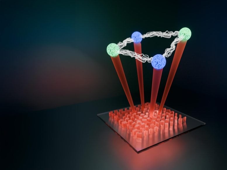
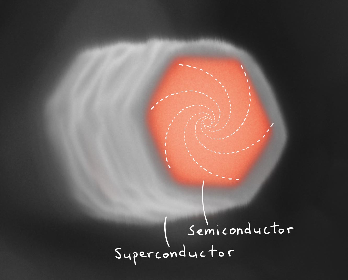
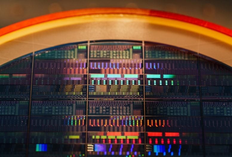
Figure 1. Quantum Computer into a Tiny Chip.
Reimagining Quantum Hardware
Traditionally, manipulating photons—the particles of light used in many quantum systems—requires intricate arrangements of waveguides, mirrors, lenses, and beam splitters. These setups allow photons to become entangled, a process essential to quantum computing and communication. But they’re also large, fragile, and complex—posing major challenges to scaling. Figure 1 shows Quantum Computer into a Tiny Chip.
Harvard’s research team, led by Federico Capasso at the John A. Paulson School of Engineering and Applied Sciences, has changed the equation. Their work, published in science, shows that a single chip-thin metasurface can perform the same quantum optical functions as an entire lab setup.
A Flat Future for Quantum Optics
The metasurface is patterned with nanoscale structures that precisely manipulate light. It enables the generation of entangled photon states and executes complex quantum operations—all within a flat, compact device.
“This represents a major step forward in solving the scalability challenge,” said Kerolos M.A. Yousef, the study’s first author. “We’ve taken a full quantum optical system and shrunk it down to a single, stable, and robust metasurface.”
Smart Design Meets Quantum Behavior
What sets this project apart is its use of graph theory to guide the design of the metasurface. This mathematical approach allowed the researchers to program complex quantum behavior into the flat surface itself, eliminating the need for numerous separate components.
Toward Scalable Quantum Devices
By significantly reducing the size, complexity, and fragility of quantum optical systems, Harvard’s metasurface technology could accelerate the development of scalable quantum computers and communication networks [1]. Funded in part by the Air Force Office of Scientific Research (AFOSR), the work paves the way for compact, practical quantum devices ready for real-world applications.
metasurfaces: A New Blueprint for Scalable Quantum Devices
The research team’s findings point to a game-changing future for optical quantum devices—one that moves beyond traditional, bulky components like waveguides, beam splitters, and even large optical chips. Instead, they envision systems built on metasurfaces: ultra-thin, nano-engineered layers that manipulate light with remarkable precision.
Unlike conventional components that require painstaking alignment and are challenging to scale, metasurfaces offer a suite of advantages:
- Resilience to external disturbances
- Simple and cost-effective fabrication
- Minimal optical loss
- No need for complex alignment
- Compact, flat form factors
The Scaling Challenge
Designing a single metasurface capable of controlling key properties of light—such as brightness, phase, and polarization—is no easy feat. The complexity grows rapidly as more photons are introduced, each adding layers of interference pathways. In traditional setups, managing this would require a sprawling array of additional beam splitters and output ports—a major scalability bottleneck.
Graph Theory: Turning Complexity into Clarity
To tackle this problem, the researchers employed a powerful mathematical tool: graph theory. By representing entangled photon states as networks of nodes and connections, they could map how photons interact and interfere. This visual, mathematical framework allowed them to predict outcomes and design the metasurfaces accordingly.
While graph theory is used in quantum computing and error correction, its application to metasurface design and operation is groundbreaking. It turns an overwhelming design problem into a solvable one—where the quantum state and the metasurface become two sides of the same design challenge.
A Collaborative Breakthrough
This research was conducted in partnership with Marko Lončar’s lab, known for expertise in quantum optics and integrated photonics, and brought together deep theoretical and experimental knowledge.
“This approach could finally solve the long-standing scalability challenge in optical quantum systems,” said Neal Sinclair, research scientist and co-author. “It also deepens our understanding of how to design metasurfaces for quantum light generation and control. Using graph theory, we’ve linked the logic of quantum behavior directly to the structure of the device itself.”
Reference:
- https://scitechdaily.com/harvard-just-collapsed-a-quantum-computer-onto-a-chip/
Cite this article:
Keerthana S (2025), Harvard Engineers Pack a Quantum Computer into a Tiny Chip, AnaTechMaz, pp.336
Recent Post
-
Blue Laser Cracks a 150-Year-Old Physics Puzzle
For more than 100 years, physicists suspected that a strange magnetic signal was present in...
-
Physicists Set New Record for Qubit Coherence, Pushing Quantum Limits
On July 8, 2025, researchers at Aalto University in Finland announced...
-

fortios: Ensuring Quantum-Safe Security in the Era of Advanced Computing
Traditional encryption has safeguarded data for years, but the emergence of...
-
Breakthrough in Measurement Tech: New System Approaches Physics' Theoretical Boundaries
Fast, precise, and field-ready—a quantum-level optical frequency...
-

New Quantum Technology May Finally Prove the Existence of the Multiverse
Imagine a gamma ray laser so precise that it can destroy cancer cells...
-
Harvard Engineers Pack a Quantum Computer into a Tiny Chip
In a breakthrough that could reshape the future of quantum technology, engineers at Harvard have developed...
-
Quantum Leap: Scientists Uncover Hidden Clue to Solving a 60-Year-Old Superconducting Puzzle
A team in Copenhagen has discovered an ingenious “backdoor” method...
-

U.S. Mathematicians Transform ‘Pure’ Math Once Deemed Impractical into a Quantum Computing Breakthrough
Researchers at the University...
-
Physicists Astonished by Groundbreaking Room-Temperature Quantum Discovery
In a groundbreaking leap for quantum science, researchers have shown ...
-

Physicists Develop a “Quantum Lie Detector” to Expose Fake Quantum Computers
Is it possible to verify whether a large quantum system genuinely follows...
-
Chinese Scientists Reveal Atom Array 10 Times Larger, Paving Way for Next-Generation Quantum Processors
Chinese scientists have made a...
-

Harnessing Sound Waves: A Breakthrough Route to Practical Quantum Computing
Caltech researchers have designed a new kind of hybrid quantum...
-
Quantum Guitar: Scientists Resolve 90-Year-Old Puzzle of the Damped Harmonic Oscillator
Imagine plucking a guitar string. It vibrates, the sound lingers, and ...
-

Scientists Create ‘World’s Smallest Cat Video’ to Push Quantum Computing Forward
A team of physicists in Shanghai has made what they call the...
Sandia Harnesses Chiplet Technology to Advance AI and Quantum Computing
Sandia has a long-standing track record in semiconductor research, driven by...