
3D Integrated Circuits
Three-dimensional (3D) integrated circuits (ICs), which contain multiple layers of active devices, have the potential to dramatically enhance chip performance, functionality, and device packing density. They also provide for microchip architecture and may facilitate the integration of heterogeneous materials, devices, and signals. However, before these advantages can be realized, key technology challenges of 3D ICs must be addressed. More specifically, the processes required to build circuits with multiple layers of active devices must be compatible with current state-of-the-art silicon processing technology. These processes must also show manufacturability, i.e., reliability, good yield, maturity, and reasonable cost. To meet these requirements, IBM has introduced a scheme for building 3D ICs based on the layer transfer of functional circuits, and many process and design innovations have been implemented. This paper reviews the process steps and design aspects that were developed at IBM to enable the formation of stacked device layers. Details regarding an optimized layer transfer process are presented, including the descriptions of 1) a glass substrate process to enable through-wafer alignment; 2) oxide fusion bonding and wafer bow compensation methods for improved alignment tolerance during bonding; 3) and a single-damascene patterning and metallization method for the creation of high-aspect-ratio (6:1 < AR < 11:1) contacts between two stacked device layers. This process provides the shortest distance between the stacked layers (<2 µm), the highest interconnection density (>10 8 vias/cm 2 ), and extremely aggressive wafer-to-wafer alignment (submicron) capability.
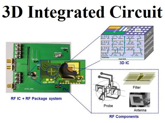
Figure 1 Three-dimensional integrated circuit
Figure 1 shows three-dimensional integrated circuit (3D IC) and 2.5D IC with Si interposer are regarded as promising candidates to overcome the limitations of Moore’s law because of their advantages of lower power consumption, smaller form factor, higher performance, and higher function density [1,2,3,4]. To achieve 3D and 2.5D IC integrations, several key technologies are required, such as through-silicon via (TSV), wafer thinning, and handling, as well as wafer/chip bonding. Since TSV provides the advantages of shortening interconnection paths and thinner package size, it is considered as the heart of 3D integration. TSV formation is categorized into three types during 3D/2.5D IC process. When TSV is formed before CMOS processes, the process progression is defined as via first. In via middle flow, backend process only continues after the completion of TSV process. The final scheme is via last where TSV is fabricated from the front side or back side of wafer after completing the CMOS processes.
The choice of TSV schemes is based on the final application requirement in the semiconductor industry. TSV technology has been developed for many applications, such as MEMS, mobile phone, CMOS image sensor (CIS), bio application devices, and memory products. Thus, a number of studies have been conducted on the manufacturing of TSV. In current status, with the relatively high fabrication cost, TSV implementation in 3D IC and advanced packaging applications is not generally implemented yet [5, 6]. In this paper, we review the important manufacturing processes of TSV and related failure modes when TSV has a smaller diameter and higher aspect ratio. Furthermore, TSV fabrication has various important processes, including via formation by deep reactive ion etching (DRIE), lining with dielectric layer, barrier and seed layers, via filling, chemical mechanical polishing (CMP), and Cu revealing process. Each key technique will be introduced in detail in the following sections.[2]
References:
- https://ieeexplore.ieee.org/document/5388751
- https://nanoscalereslett.springeropen.com/articles/10.1186/s11671-017-1831-4
Cite this article:
Thanusri swetha J (2021), 3D Integrated Circuit, Anatechmaz, pp. 24
Recent Post
-

A Review of Chatbot Technology
A chatbot is an artificial intelligence (AI) software that can simulate a conversation (or a chat) with a user in natural language...
-
The Future Technologies of Extended reality (XR) in HealthCare
Extended reality (XR) is one of the key technologies shaping up the future of healthcare...
-

An Overview of Facial Recognition System
A facial recognition system is a technology capable of matching a human face from a digital image...
-

The Evolution of Internet of Medical Things (IoMT) in Healthcare
The IoMT market consists of smart devices, such as wearables...
-
The Features of Moorebot Scout: AI-Powered Autonomous
Scout is the world-first autonomous home robot for intelligent surveillance...
-
An Emerging Technology: Nanorobotics
Nanorobotics is an emerging technology field creating machines or robots whose components...
-

An Overview: The Internet of Medical Things (IoMT)
The Internet of Medical Things (IoMT) is the network of Internet-connected medical devices...
-
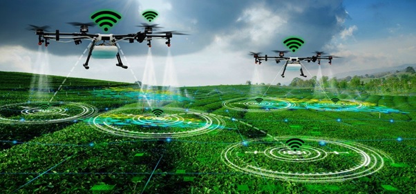
The Internet of Things in Agriculture
The Internet of Things (IoT) is about making “dumb” things “smart” by connecting them to each other...
-
3D Integrated Circuits
Three-dimensional (3D) integrated circuits (ICs), which contain multiple layers of active devices, have the potential...
-
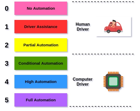
Artificial intelligence in self-driving cars
A self-driving car (sometimes called an autonomous car or driverless car) is a vehicle that uses a combination...
-
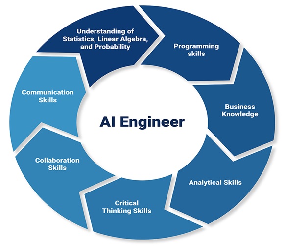
AI Engineering
An artificial intelligence engineer is an individual who works with traditional machine learning techniques...
-
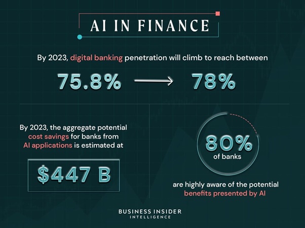
Artificial intelligence in Finance
AI and the finance industry are a match made in heaven. The financial sector relies on accuracy, real-time reporting and processing...
-

Internet of Behaviours (IOB)
Internet of Behaviours (IOB) aims to discuss how data are better understood and used to construct and promote...
-
Machine Learning towards Intelligent Systems
The emergence and continued reliance on the Internet and related technologies has resulted in the generation...
-
Tactile Virtual Reality
Innovative technologies offer more immersive experiences like AR and VR. Virtual Reality immerses the user in a simulated...