
The Technology Of 5nm Processor
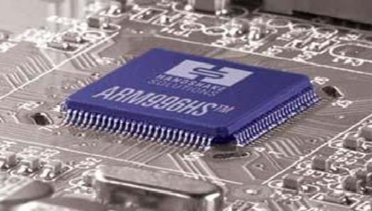
The 5nm (nanometer) processor technology represents a major advancement in semiconductor manufacturing, enabling faster, more power-efficient, and densely packed chips. It’s part of a long trend in miniaturizing transistors—the building blocks of processors—allowing more to be placed on a single chip. Here's a breakdown of what makes 5nm processors technologically significant: Figure 1 shows Inside the Breakthrough Technology of 5nm Processors
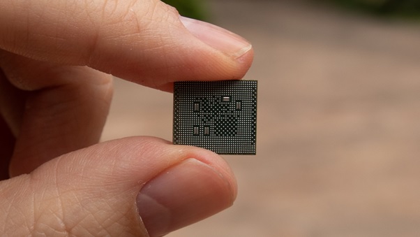
Figure 1. Inside the Breakthrough Technology of 5nm Processors.
What Does "5nm" Mean?
- "5nm" refers to the process node, which is a marketing term used by semiconductor companies. It used to relate to the actual gate length of a transistor, but today it's more symbolic of each new generation of technology.
- At 5nm, billions of transistors can fit into a chip the size of a fingernail—up to 171 million transistors per mm², compared to 96 million per mm² in 7nm chips.
Key Technologies Behind 5nm Chips:
- 5nm chips use EUV lithography for precise patterning of transistors on silicon wafers.
- EUV has a wavelength of 13.5nm, enabling finer details and more accurate etching than traditional DUV (Deep Ultraviolet).
- Most 5nm chips still use FinFET (Fin Field-Effect Transistors), which are 3D transistors that reduce power leakage./li>
- Some advanced variants explore GAAFETs (Gate-All-Around FETs), which further improve control over current flow.
- Smaller transistors reduce resistance and capacitance, allowing higher frequencies (speed) and lower power consumption.
- Enables better performance for mobile devices, data centers, AI, and edge computing.
1.Extreme Ultraviolet Lithography (EUV)
2.FinFET or Nanosheet Transistors
3.Increased Density and Performance
Real-World Examples:
- Apple A14 Bionic (in iPhone 12): First commercial 5nm chip.
- Apple M1 / M1 Pro / M1 Max: Desktop-class performance in a mobile chip.
- AMD Zen 4 & NVIDIA chips: Incorporate TSMC’s 5nm process for better gaming and server performance.
- Qualcomm Snapdragon 8 Gen 1 and Samsung Exynos 2100 also use 5nm nodes.
Challenges in 5nm Technology:
- Cost: Manufacturing 5nm chips is expensive; fabs cost billions.
- Design Complexity: Needs advanced software tools and longer design cycles.
- Thermal Management: More transistors = more heat in smaller areas.
What’s Next After 5nm?
- The industry is moving to 3nm and 2nm nodes.
- New architectures like GAAFET, chiplets, and 3D stacking are being explored to sustain Moore’s Law.
Reference:
- https://semiconductor.samsung.com/news-events/news/samsung-introduces-the-industrys-first-5nm-processor-powering-the-next-generation-of-wearables/
Cite this article:
Vinotha D (2021), The Technology Of 5nm Processor, AnaTechMaz, pp. 31
Recent Post
-
The Technology of 5nm Processor
The 5nm (nanometer) processor technology represents a major advancement in semiconductor...
-

AI in Cloud Computing
AI in Cloud Computing is the integration of artificial intelligence (AI) capabilities into cloud...
-

AI shopping system
An AI shopping system is a technology-driven solution that uses artificial...
-

An Overview of Artificial Eye
An artificial eye is a technological device designed to restore or enhance vision in....
-
Blue Brain Technology
The Blue Brain Project was a Swiss neuroscience initiative launched in May 2005 at EPFL....
-

Camera Motion Sensor System
A Camera Motion Sensor System is a surveillance or monitoring system that combines a camera....
-
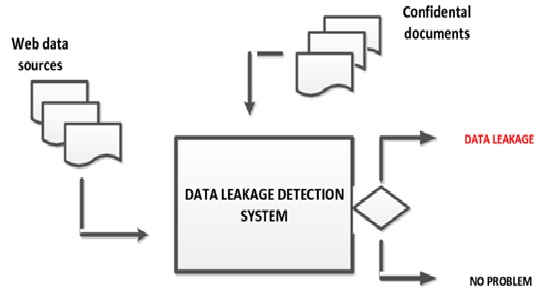
Data Leakage Detection System
A Data Leakage Detection System is a security mechanism designed to identify, monitor, and....
-
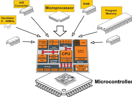
Difference Between Microprocessor and Microcontrollers
A microprocessor is essentially the brain of a computer system—it is a central processing...
-

Features of Electronic Eye Circuit
An Electronic Eye Circuit mimics the function of a human eye by detecting changes in light.....
-

Generative Artificial Intelligence (AI)
Generative AI refers to a subset of artificial intelligence techniques that enable machines....
-
Overview of Clockless Chips
Clockless chips, also known as asynchronous chips, represent a shift from traditional.....
-
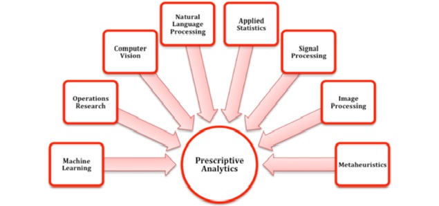
The Methods of Prescriptive Analytics
Prescriptive analytics is the phase of data analytics focused on recommending specific actions...
-
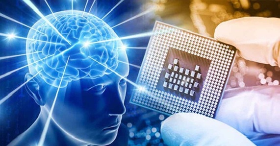
The Artificial Neurons on Silicon Chips
In 2021, scientists made a breakthrough in developing artificial neurons built on silicon chips...
-

The Invention of Crypto Currency
Cryptocurrency wasn’t actually invented in 2021 — it began much earlier — but 2021 was a landmark...
-
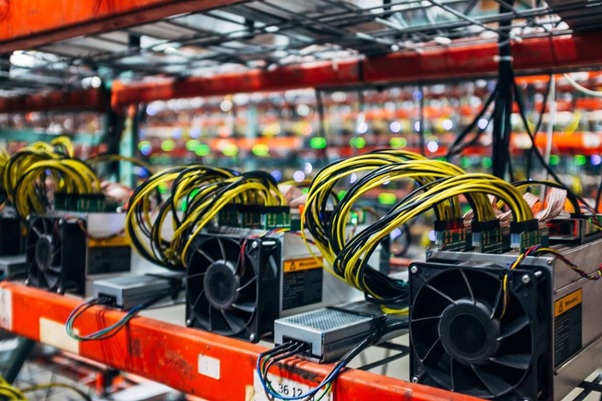
The Platform of Bitcoin Mining
Bitcoin mining is the process by which new bitcoins are created and transactions are verified.....