University of Sydney Nano Institute Unveils Breakthrough Silicon Photonics Chip
In a groundbreaking development, researchers at the University of Sydney Nano Institute have introduced a cutting-edge silicon semiconductor chip that seamlessly integrates electronics with photonic components, harnessing the power of light to significantly expand radio-frequency (RF) bandwidth. This technological leap not only enhances the chip's capacity to handle more information but also introduces advanced filter controls, marking a major stride in semiconductor innovation.
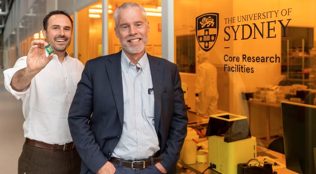
Figure 1. The Sydney Nanoscience Hub. (Credit: Stefanie Zingsheim)
Figure 1 shows Dr Alvaro Casas Bedoya, holding the new chip, with Professor Ben Eggleton in the Sydney Nanoscience Hub. The compact chip, constructed using emerging silicon photonics technology, boasts the integration of diverse systems on semiconductors less than 5 millimeters wide. Pro-Vice-Chancellor (Research) Professor Ben Eggleton likens the process to assembling Lego building blocks, where new materials are intricately integrated through advanced packaging of electronic 'chiplets.'
The implications of this invention are vast, with potential applications ranging from advanced radar and satellite systems to wireless networks. Moreover, it is anticipated to play a pivotal role in the advent of 6G and 7G telecommunications, heralding a new era of connectivity. The chip's versatility could also extend to fostering advanced sovereign manufacturing, particularly in high-tech value-add factories.
Published in Nature Communications, the research behind this revolutionary chip was led by Dr. Alvaro Casas Bedoya, Associate Director for Photonic Integration in the School of Physics. He emphasizes that the unique method of heterogeneous materials integration took a decade to perfect. The collaboration with overseas semiconductor foundries, combined with local research infrastructure and manufacturing, has been instrumental in developing this photonic integrated circuit.
Professor Eggleton underscores the critical role of semiconductors in technologies listed by the Federal Government as being in the National Interest. This breakthrough aligns with initiatives like the Semiconductor Sector Service Bureau (S3B), sponsored by the NSW Government, which aims to bolster the local semiconductor ecosystem.
Dr. Nadia Court, Director of S3B, applauds the work, stating that it aligns with their mission to advance semiconductor technology in Australia. The innovation reinforces local strength in research and design at a time when there is a heightened global focus and investment in the semiconductor sector.
The integrated circuit, a collaboration with scientists at the Australian National University, was crafted at the Core Research Facility cleanroom at the University of Sydney Nanoscience Hub—a purpose-built $150 million facility with state-of-the-art lithography and deposition capabilities.
The chip's photonic circuit delivers an impressive 15 gigahertz bandwidth of tunable frequencies, with spectral resolution down to just 37 megahertz. This remarkable achievement, spearheaded by PhD student Matthew Garrett, represents a significant leap in microwave photonics and integrated photonics research.
Co-author and Senior Research Fellow Dr. Moritz Merklein envisions a new generation of compact, high-resolution RF photonic filters with wideband frequency tunability. This breakthrough opens doors to enhanced communications and sensing capabilities, particularly beneficial in air and spaceborne RF communication payloads.
In essence, the University of Sydney Nano Institute's silicon photonics chip marks a transformative moment in semiconductor technology, propelling Australia into a position of strength on the global stage. The potential applications across various industries promise a future where connectivity is not just efficient but revolutionary.
Source: University of Sydney
Cite this article:
Hana M (2023), University of Sydney Nano Institute Unveils Breakthrough Silicon Photonics Chip, AnaTechMaz, pp. 302


