Nanoscale Transistors Have the Potential to Make Electronics More Efficient
Researchers are utilizing quantum mechanical properties to address the limitations of silicon semiconductor technology. Silicon transistors, essential for amplifying and switching signals in most electronic devices—from smartphones to automobiles—face a fundamental physical limit that restricts their ability to operate below a certain voltage.
Known as the "Boltzmann tyranny," this limit impedes the energy efficiency of computers and other electronics, posing a challenge with the rapid advancement of artificial intelligence technologies that require faster computation. To address this constraint in silicon, MIT researchers developed a novel three-dimensional transistor using a distinctive combination of ultrathin semiconductor materials.

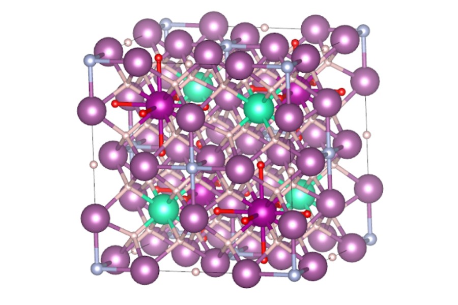
Figure 1. Nanoscale Transistors for Enhanced Electronics Efficiency
The researchers' devices, built with vertical nanowires just a few nanometers in width, achieve performance on par with the latest silicon transistors but operate effectively at significantly lower voltages than traditional devices. "This technology has the potential to replace silicon, enabling all the current functionalities of silicon with greatly improved energy efficiency," explains Yanjie Shao, an MIT postdoc and lead author of a paper on these innovative transistors. Figure 1 shows Nanoscale Transistors for Enhanced Electronics Efficiency.
These transistors exploit quantum mechanical properties to achieve both low-voltage operation and high performance within a footprint of just a few square nanometers. Their tiny size allows more 3D transistors to be integrated onto a single chip, paving the way for faster, more powerful, and energy-efficient electronics.
“With conventional physics, there’s a limit to how far we can push,” says senior author Jesús del Alamo, the Donner Professor of Engineering in MIT’s Department of Electrical Engineering and Computer Science (EECS). “Yanjie’s work demonstrates that we can surpass that limit by employing different physics. While there are still challenges to make this approach commercially viable, it’s a genuine breakthrough in concept.”
The study’s authors also include Ju Li, the Tokyo Electric Power Company Professor in Nuclear Engineering and a professor of materials science and engineering at MIT; EECS graduate student Hao Tang; MIT postdoc Baoming Wang; and professors Marco Pala and David Esseni from the University of Udine in Italy.
Going Beyond Silicon
In electronic devices, silicon transistors commonly function as switches. When a voltage is applied, electrons move across an energy barrier from one side of the transistor to the other, switching it from “off” to “on” and allowing it to represent binary digits for computation.
A transistor’s switching slope measures the sharpness of this “off” to “on” transition. The steeper the slope, the less voltage required to activate the transistor, improving energy efficiency. However, due to the nature of electron movement across energy barriers, the phenomenon known as Boltzmann tyranny imposes a minimum voltage needed to switch a transistor at room temperature.
To bypass this physical limit, MIT researchers adopted a different set of semiconductor materials—gallium antimonide and indium arsenide—and designed their devices to exploit a unique quantum mechanical effect known as quantum tunneling. Quantum tunneling allows electrons to pass through barriers. The team created tunneling transistors that encourage electrons to penetrate the energy barrier, rather than going over it.
“This makes it easy to turn the device on and off,” Shao explains. Although tunneling transistors can enable sharp switching slopes, they generally operate with low current, which limits device performance. To achieve powerful transistor switches for demanding applications, higher current is needed.
Precision Fabrication
Using tools at MIT.nano, MIT’s advanced facility for nanoscale research, engineers precisely controlled the 3D geometry of their transistors, creating vertical nanowire heterostructures with a diameter of just 6 nanometers—believed to be the smallest 3D transistors to date.
This precision allowed them to achieve both sharp switching slopes and high current, thanks to quantum confinement, a phenomenon that alters electron properties in confined spaces. The small size of the transistors enabled a strong quantum confinement effect and a thin tunneling barrier.
“Designing these material heterostructures gives us the flexibility to create a very thin tunneling barrier, which leads to high current,” Shao explains. Fabricating such small devices was a major challenge. “We’re working with single-nanometer dimensions, and few groups can produce transistors this small,” says del Alamo.
Their devices exceeded conventional silicon transistors in performance, achieving a switching slope below the fundamental limit of silicon and performing 20 times better than similar tunneling transistors. “This is the first time we’ve achieved such sharp switching steepness with this design,” says Shao.
The team is now focused on refining their fabrication techniques to ensure uniformity across entire chips. Even a 1-nanometer variance can impact electron behavior and device performance. They’re also investigating vertical fin-shaped structures to further improve device uniformity.
“This work marks a significant step forward in improving broken-gap tunnel field effect transistor (TFET) performance, demonstrating steep slopes and record drive current,” says Aryan Afzalian of imec, who was not involved in the research.
Source:MIT News
Cite this article:
Janani R (2024), Nanoscale Transistors Have the Potential to Make Electronics More Efficient, AnaTechMaz, pp. 72


