
Chip-Based Terahertz Wave System Could Enhance Efficiency and Sensitivity in Electronics
MIT researchers have developed a chip-based terahertz wave generator that achieves higher radiating power without the need for bulky silicon lenses. Terahertz waves, which have shorter wavelengths and higher frequencies than radio waves, enable faster data transmission, more precise medical imaging, and higher-resolution radar.
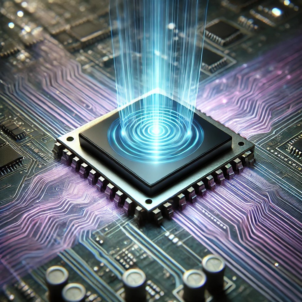
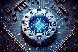
Figure 1. Advanced Chip Technology Boosts Terahertz Wave Efficiency and Sensitivity.
Generating these waves efficiently on a semiconductor chip has been challenging due to insufficient radiating power. Traditional methods often require large, expensive silicon lenses that hinder device integration. Figure 1 shows Advanced Chip Technology Boosts Terahertz Wave Efficiency and Sensitivity.
To address this, the researchers designed a terahertz amplifier-multiplier system. By attaching a thin, patterned sheet to the chip's back and using higher-power Intel transistors, they created a more efficient and scalable solution.
This compact technology could power terahertz arrays for enhanced security scanners, environmental monitoring, and other advanced applications.
Scalable Terahertz Chip Paves the Way for Advanced Electronics
MIT researchers have developed a scalable, chip-based terahertz wave generator that eliminates the need for bulky silicon lenses, making it more practical for integration into electronic devices. Terahertz waves, which have shorter wavelengths and higher frequencies than radio waves, enable faster data transmission, precise medical imaging, and high-resolution radar.
Traditional semiconductor-based terahertz sources struggle with low radiating power unless paired with large, expensive lenses, limiting their use in compact electronics. To address this, the researchers designed a terahertz amplifier-multiplier system, utilizing a thin, patterned material sheet on the chip’s back and high-power Intel transistors to boost efficiency.
“For a terahertz array with hundreds of chips, there is no space for silicon lenses. We needed a different approach, and we’ve demonstrated a promising solution for scalable, low-cost terahertz arrays,” says lead author Jinchen Wang, a graduate student in MIT’s Department of Electrical Engineering and Computer Science (EECS).
Wang collaborated with EECS graduate students Daniel Sheen and Xibi Chen, T.J. Rodgers RLE Laboratory managing director Steven F. Nagle, and senior author Ruonan Han, an associate professor leading MIT’s Terahertz Integrated Electronics Group. The research will be presented at the IEEE International Solid-State Circuits Conference.
Overcoming Transmission Barriers in Terahertz Wave Generation
Terahertz waves, which occupy the electromagnetic spectrum between radio waves and infrared light, offer high data capacity and the ability to penetrate various materials more effectively than infrared
A Scalable Approach to Terahertz Wave Generation
To create an efficient and scalable terahertz wave source, MIT researchers developed a cost-effective method to overcome transmission barriers. They selected a commercially available substrate material with a dielectric constant close to the desired level for matching—the process of equalizing the dielectric constants of silicon and air to minimize signal reflection.
To fine-tune the material, they used a laser cutter to create tiny subwavelength holes, effectively lowering the dielectric constant by introducing air pockets. “Since the dielectric constant of air is 1, cutting holes in the sheet is equivalent to injecting air, which reduces the overall dielectric constant,” explains lead researcher Jinchen Wang.
In addition to this innovative matching sheet, the team integrated high-performance transistors developed by Intel, which feature a higher maximum frequency and breakdown voltage than standard CMOS transistors.
“These two things taken together—the more powerful transistors and the dielectric sheet—plus a few other small innovations, enabled us to outperform several other devices,” Wang says.
The resulting chip achieved a peak radiation power of 11.1 decibel-milliwatts, surpassing state-of-the-art techniques. Importantly, the chip is low-cost and scalable, making it feasible for integration into real-world electronic devices.
light. However, efficiently generating these waves using semiconductor chips has been a persistent challenge.
A common approach involves using a CMOS chip-based amplifier-multiplier chain to boost radio waves into the terahertz range. Ideally, these waves would pass through the silicon chip and emit cleanly into the open air. However, a property known as the dielectric constant disrupts this process.
Silicon’s high dielectric constant causes most terahertz waves to reflect at the silicon-air boundary rather than transmitting through, leading to significant signal loss. Traditional solutions rely on bulky silicon lenses to enhance the remaining signal strength, but these lenses hinder scalability.
MIT researchers took a different approach, leveraging an electromechanical principle known as matching. By affixing a thin sheet of material with a dielectric constant between silicon and air to the back of the chip, they significantly reduced signal reflection. This innovative matching layer allows most terahertz waves to be efficiently transmitted, eliminating the need for large external lenses.
This breakthrough enables more scalable and efficient terahertz arrays, paving the way for improved high-speed communication, medical imaging, and security scanning technologies.
Source: MIT NEWS
Cite this article:
Priyadharshini S (2025),Chip-Based Terahertz Wave System Could Enhance Efficiency and Sensitivity in Electronics, AnaTechMaz, pp. 209
Recent Post
-

Scientists Discover a New Method to Control Electrons: The Quantum Twist
A promising alternative approach, investigated in recent years...
-

Physicists Discover a Hidden Quantum Realm Within the Proton – And It’s Stranger Than We Imagined
The proton’s interior is one of the most dynamic and elusive.....
-

Scientists Achieve Historic Breakthrough by Linking Quantum Processors, Paving the Way for Scalable Supercomputers
In a groundbreaking advancement for large-scale quantum computing, researchers...
-

The Quantum Blueprint: Unraveling How Photosynthesis Defies Classical Physics
Engineers have long sought efficient methods to convert solar energy...
-

Quantum Computers Receive a Major Boost with Fiber-Optic Technology
Following a year of rapid growth, quantum computing stocks experienced...
-

Quantum Computing Advancements Edge Us Nearer to Universal Simulation
Physicists at Google’s laboratory, in collaboration with researchers from PSI’s Center f...
-

Quantum Imaging Advances: Now Faster, Smaller, and More Precise
Researchers from the ARC Centre of ...
-

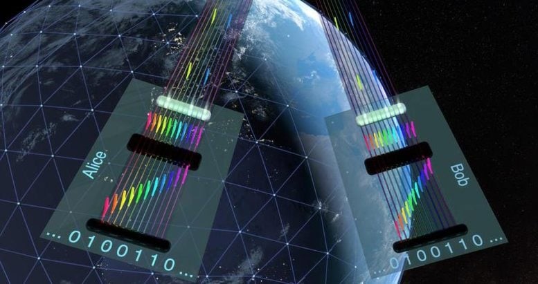
Quantum Networking Milestone: Entangled Photons Maintain Transmission for Over 30 Hours
This achievement marks a significant step toward a functional quantum internet, which...
-
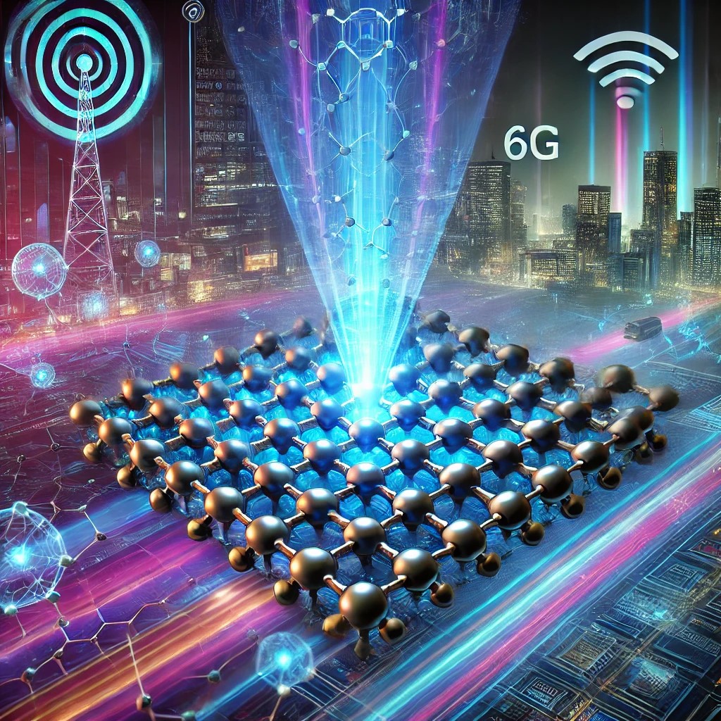
Scientists Discover a New Method to Boost Wireless Speeds Using Graphene
A research team from the University of Ottawa has made significant strides in...
-
Quantum Encryption Breakthrough Harnesses Light and Color for An Unhackable Internet
The future of internet security is at risk as quantum computers may one day crack...
-

Scientists Boost the Universe’s Weakest Signals 1,000x To Uncover Dark Matter
If dark matter exists, its interactions with ordinary matter are so weak that even the...
-
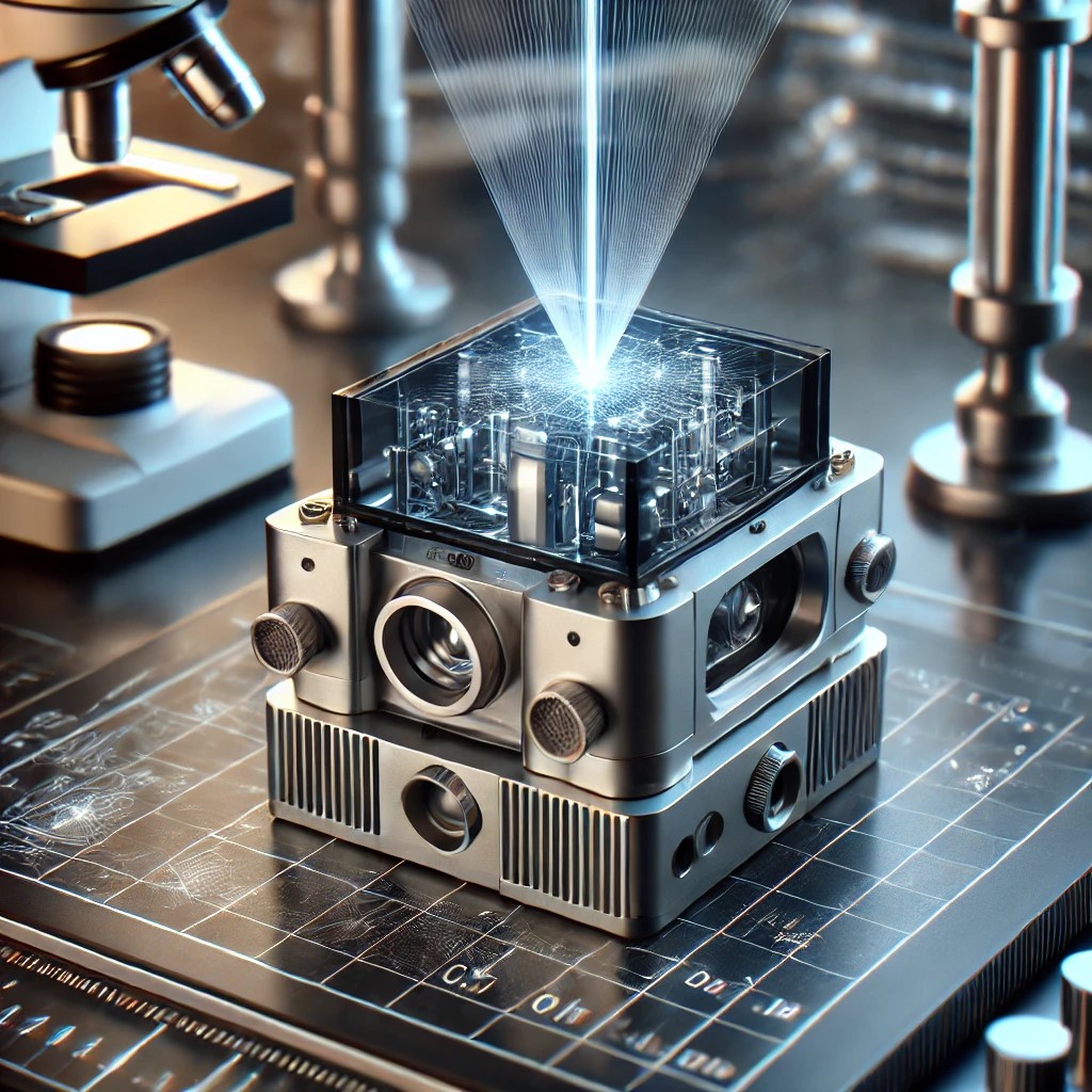
This Compact Device Captures and Measures Light in an Unprecedented Way
Researchers have developed a groundbreaking method to trap and measure light...
-

Magnetism Solves a Major Challenge in Quantum Technology
"While two-dimensional (2D) materials exhibit remarkable functionalities...
-
Chip-Based Terahertz Wave System Could Enhance Efficiency and Sensitivity in Electronics
MIT researchers have developed a chip-based terahertz wave generator that ...
-
Quantum Revolution: Capturing Atoms on a Microchip
By integrating photonics to miniaturize cold atom trapping, researchers are ...