Electron Beams Redefine Microchip Manufacturing at the Nanoscale
Electronic devices have become so deeply integrated into daily life that we often overlook the complexity behind their design. Take a smartphone, for instance—its seamless functionality depends on countless tiny components working in perfect synchrony. Among these hidden elements are radio frequency (RF) filters, which are essential for ensuring devices correctly receive signals over Wi-Fi and mobile networks. These filters often rely on piezoelectric thin films—special materials that generate electricity when stressed and change shape when an electric field is applied.

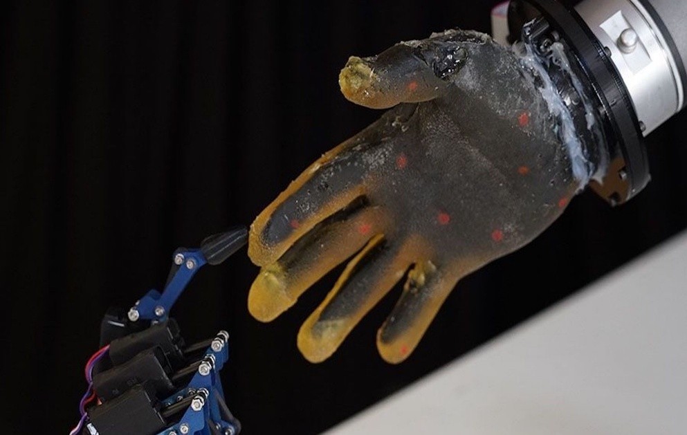
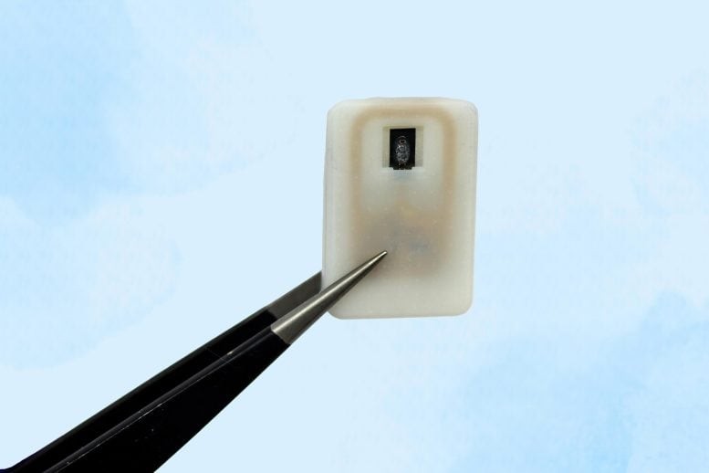
Figure 1. Microchip Manufacturing.
But piezoelectric thin films do much more than support wireless communication. They are critical in sensors, actuators, and miniature energy-harvesting devices, and are now being investigated for applications in cutting-edge fields like quantum technologies. All of these uses require extremely high-quality thin films—something that depends on both the materials chosen and the precision of the fabrication process.
Now, researchers at Empa’s Surface Science & Coating Technologies lab have developed a breakthrough deposition method for these thin films. Their new technique enables the creation of high-performance piezoelectric layers on insulating substrates at relatively low temperatures—a first in the field. Their work has been published in Nature Communications and a patent application is underway.
Reinventing a Known Process with New Precision
The team began with a technique called HiPIMS (High Power Impulse Magnetron Sputtering), a widely used method in thin-film production. In this process, atoms are ejected from a solid material (the "target") and deposited onto a surface (the "substrate") using bursts of high-energy plasma. When gases like argon are used in the plasma, their ions bombard the target, releasing atoms that coat the substrate.
HiPIMS differs from standard sputtering by using pulsed energy bursts, which ionize many of the atoms as they fly through the plasma [1]. This makes it possible to accelerate ions toward the substrate by applying a negative voltage—ideal for producing dense, high-quality coatings. Figure 1 represents microchip manufacturing.
However, this method previously wasn’t suitable for piezoelectric thin films. That’s because it accelerates not only the desired target ions but also undesirable argon ions, which can contaminate the film and compromise performance. Even small levels of argon can lead to failure in piezoelectric devices that operate under high voltage.
Timing Is Everything: A Smart Solution
Despite this challenge, the Empa team saw potential in HiPIMS for piezoelectric materials. The key was to selectively accelerate only the desired ions. During his PhD research, Jyotish Patidar developed an elegant timing strategy: the researchers discovered that argon ions typically arrive at the substrate before the target ions do. By carefully timing the voltage pulse applied to the substrate, they could allow the argon ions to pass unaccelerated and then apply voltage just in time to accelerate only the target ions.
This clever adjustment made it possible to produce high-purity, high-performance piezoelectric thin films—on par with or even better than those made using conventional techniques.
Turning the “Electron Shower” into a Tool
The next challenge was coating insulating substrates, such as glass or sapphire, which can't carry an electric voltage. In typical setups, this would make ion acceleration impossible or lead to argon contamination.
The Empa team devised a unique workaround using a phenomenon known as the “electron shower.” Each time the magnetron fires a pulse, it doesn’t just eject ions—it also sends out a stream of fast-moving electrons. When these electrons hit the insulating substrate, they temporarily charge it negatively. If the researchers time the next pulse correctly, this negative charge can help accelerate only the target ions toward the substrate—without the need for direct voltage.
This technique, dubbed Synchronized Floating Potential HiPIMS (SFP-HiPIMS), allows high-quality piezoelectric films to be deposited on both conductive and insulating substrates at low temperatures—a major advantage for semiconductor manufacturing, where high heat is often a barrier.
A New Frontier for Thin Films
“With our method, we were able to produce piezoelectric thin films on insulating substrates just as well as on conductive ones,” says Empa researcher Sebastian Siol. This capability is especially important for the semiconductor industry, where many production tools don’t allow for voltage application to the substrate at all.
Looking ahead, the Empa team plans to explore ferroelectric thin films, which are central to next-generation electronics, and expand into applications like photonics and quantum computing. They also aim to further optimize their process using machine learning and high-throughput experimentation.
With this breakthrough, thin-film electronics have taken a major step forward—opening the door to smarter, more efficient, and more versatile microelectronic systems.
Reference:
- https://www.nature.com/articles/s41467-025-59911-y
Cite this article:
Keerthana S (2025), Electron Beams Redefine Microchip Manufacturing at the Nanoscale, AnaTechMaz, pp.352


