
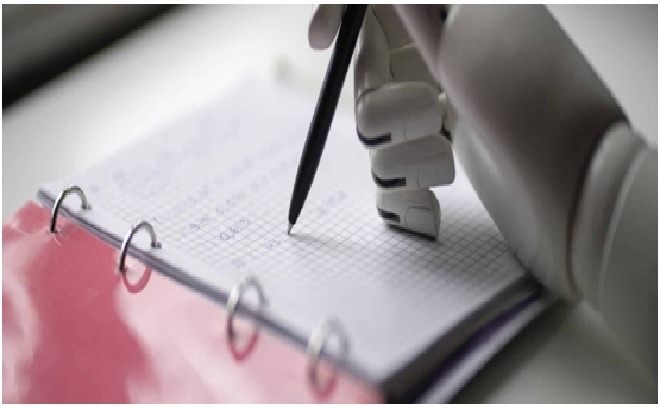
New Integration Route for Tiny Transistors
Researchers from UNSW Sydney have developed a tiny, transparent, and flexible material to be used as a novel dielectric (insulator) component in transistors. The new material would enable what conventional silicon semiconductor electronics cannot do—get any smaller without compromising their function.
The research indicates the potential for large-scale production of a 2D field-effect transistor—a device used to control current in electronics. The new material could help overcome the challenges of nanoscale silicon semiconductor production for dependable capacitance (electrical charge stored) and efficient switching behavior. [1]
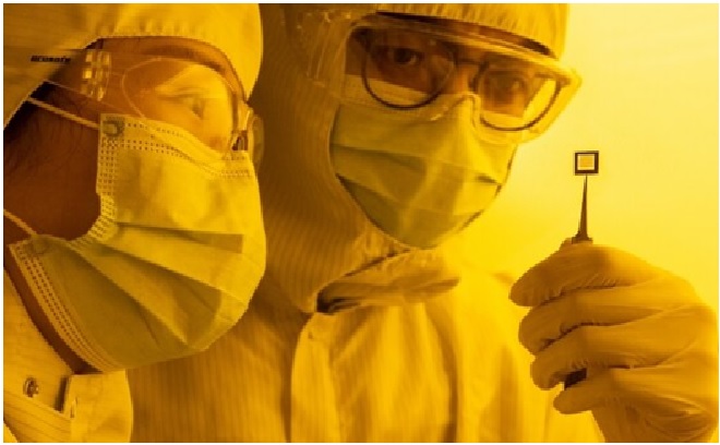
Figure 1. New Integration Route for Tiny Transistors
Figure 1 shows according to the researchers, this is one of the crucial bottlenecks to solve for the development of a new generation of futuristic electronic devices, from augmented reality, flexible displays and new wearables, as well as many yet-discovered applications.
“Not only does it pave a critical pathway to overcome the fundamental limit of the current silicon semiconductor industry in miniaturisation, but it also fills a gap in semiconductor applications due to silicon’s opaque and rigid nature,” says Professor Sean Li, UNSW Materials and Manufacturing Futures Institute (MMFI) Director and principal investigator on the research. “Simultaneously, the elastic and slim nature could enable the accomplishment of flexible and transparent 2D electronics.” [2]
Solving the semiconductor scaling issue
A transistor is a small semiconductive device used as a switch for electronic signals, and they are an essential component of integrated circuits. All electronics, from flashlights to hearing aids to laptops, are made possible by various arrangements and interactions of transistors with other components like resistors and capacitors.
Microelectronic devices continue to diminish in size to achieve higher speeds. As this shrinkage occurs, design parameters are impacted in such a way that the materials currently being used are pushed to their limits because of energy loss and dissipation as signals pass from one transistor to the next. The current smallest transistors made of silicon-based semiconductors are 3 nanometres.
To get an idea of just how small these devices need to be – imagine one centimetre on a ruler and then count the 10 millimetres of that centimetre. Now, in one of those millimetres, count another one million tiny segments – each of those is one nanometre or nm. [3]
References:
- https://www.eletimes.com/new-integration-route-for-tiny-transistors
- https://indiaeducationdiary.in/university-of-new-south-wales-engineers-develop-new-integration-route-for-tiny-transistors/
- https://www.unsw.edu.au/news/2022/08/engineers-develop-new-integration-route-for-tiny-transistors
Cite this article:
Thanusri swetha J (2022), New Integration Route for Tiny Transistors, AnaTechMaz, pp.164
Recent Post
-
New Aquatic Artificial Vision System Inspired by Crabs
Researchers at the Institute for Basic Science (IBS), Seoul National University...
-

Overview of AI is changing IoT
IoT has seen steady adopted across the business world over the past decade...
-
Using artificial intelligence to control digital manufacturing
MIT researchers have automated the process to determine ideal parameters...
-

New Textile Vest Sensor Technology to Record Lung Noises
Researchers from the Fraunhofer Institute for Ceramic Technologies and...
-
Smaller, Cheaper Lidar with New Chip-Based Beam Steering Device
Researchers have developed a new chip-based beam steering technology...
-

New Cancer Imaging Tool Combined with OCT and AI
A research team from the lab of Quing Zhu, the Edwin H. Murty Professor...
-
Advanced New Sensors could Transform Prosthetics and Robotic Limbs
The innovative research project aspires to develop sensors that provide enhanced...
-
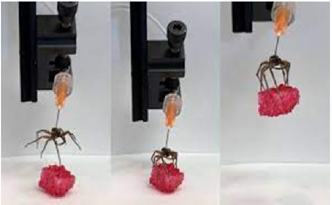
Necrobotics – Transformation of Dead Spiders into Robotic Gripping Claws
Rice University who successfully transformed dead spiders into robotic...
-

A 'nano-robot' built entirely from DNA to explore cell processes
A nano-robot constructed entirely from DNA may sound like science fiction, but it’s the...
-
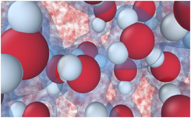
In simulation of water freezes, artificial intelligence breaks the ice
The team, based at Princeton University, accurately modeled the early stages...
-
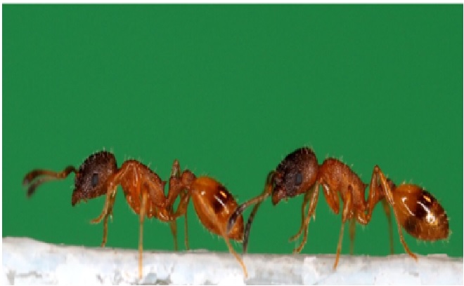
Robot helps reveal how ants pass on knowledge
Scientists have developed a small robot to understand how ants teach one another...
-

A Flashover (AI) Prediction may Rescue Firefighters
Researchers on the Nationwide Institute of Requirements and Know-how...
-

New 3D Printed Material can Sense their Own Movements
MIT researchers have created an approach for 3D printing products with tunable...
-
New Integration Route for Tiny Transistors
Researchers from UNSW Sydney have developed a tiny, transparent, and flexible...
-

AI System used to Detect Sepsis Symptoms Earlier
Researchers at Johns Hopkins developed an AI system that reduces the risk of...