
Researchers Discover “Mouse Bite” Flaws Hidden Within Computer Chips
For decades, tiny imperfections have posed major challenges for the semiconductor industry. As computer chips have grown more sophisticated and their components have shrunk to the scale of individual atoms, even the smallest structural irregularities can significantly impact performance.

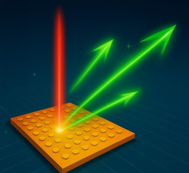
Figure 1. Scientists Reveal Tiny ‘Mouse Bite’ Defects Inside Computer Chips.
At the heart of every chip lies the transistor, a minuscule switch that regulates the flow of electricity. Each transistor has a channel that opens and closes to allow electrons to pass through. Figure 1 shows Scientists Reveal Tiny ‘Mouse Bite’ Defects Inside Computer Chips.
“The transistor is like a tiny pipe for electrons instead of water,” explained Muller. “If the walls of the pipe are rough, it slows things down. So now, measuring which walls are smooth and which are flawed is more important than ever.”
Modern high-performance chips can house billions of transistors. These days, a transistor channel may be only 15 to 18 atoms wide, making it extremely difficult to measure accurately.
From Early Transistors to 3D Chip Architectures
Muller’s career in semiconductor research dates back to his time at Bell Labs from 1997 to 2003, where transistors were originally developed. During that period, he investigated the physical limits that determine how small a transistor can be.
In the early days, transistors were laid out flat, spreading across the chip surface. As space became constrained, engineers began stacking transistors vertically, giving rise to complex three-dimensional structures.
“The challenge is that these 3D structures are smaller than a virus. Today, they’re even tinier—more like the scale of molecules inside a cell,” Muller explained.
The Rise of Advanced Electron Microscopy
While at Bell Labs, Muller and colleague Glen Wilk ’90, now vice president of technology at ASM, worked on replacing silicon dioxide—which leaked too much current at small scales—with hafnium oxide as a gate material. Their research ultimately helped establish hafnium oxide as the industry standard for computers and smartphones in the mid-2000s.
The “jet” he refers to is electron ptychography, a sophisticated computational imaging technique. It relies on an electron microscope pixel array detector (EMPAD), co-developed by Muller’s team, to capture detailed electron scattering patterns as electrons pass through a transistor.
By analyzing shifts in these patterns between scan points, scientists can reconstruct images with extraordinary clarity. The detector is so precise that it has produced the highest-resolution images ever recorded, revealing atomic arrangements in unprecedented detail—a feat recognized by Guinness World Records.
Detecting “Mouse Bite” Defects
More than 25 years after their initial collaboration, Muller and Wilk reunited, this time with support from TSMC and its Corporate Analytical Laboratories group, aiming to apply EMPAD technology to modern semiconductor devices.
“You can think of this imaging technique like solving a massive puzzle—both in collecting experimental data and performing computational reconstruction,” said Karapetyan.
Once the data were processed, the team traced the positions of individual atoms and identified subtle roughness along transistor channels. Karapetyan dubbed these tiny irregularities “mouse bites.” The defects emerged during the optimized growth process used to manufacture the structures, with test samples produced at the nanoelectronics research center Imec.
“Fabrication of modern devices involves hundreds, if not thousands, of steps—chemical etching, deposition, heating—and each step alters the structure,” Karapetyan explained. “In the past, you relied on projective images to infer what was happening. Now, we have a direct probe that lets us see after every step. For example, if I set the temperature this high, I can now directly observe how the structure responds.”
Source: SciTECHDaily
Cite this article:
Priyadharshini S (2026), Researchers Discover “Mouse Bite” Flaws Hidden Within Computer Chips, AnaTechMaz, pp. 453
Recent Post
-

Tiny Nanolaser Breakthrough Could Transform the Future of Computing
Researchers have developed an ultra-compact nanolaser that could fundamentally ...
-
Microscopic Spotlight Effect Achieved with Ultra-Thin Device
The device developed at CUNY is the first to combine two key advantages for nonlinear light ...
-
Researchers Discover “Mouse Bite” Flaws Hidden Within Computer Chips
For decades, tiny imperfections have posed major ...
-

Physicists Discover Big Bang’s Primordial Matter Behaved Like a Liquid
Quark–gluon plasma (QGP) is believed to be the very first ...
-

Scientists Create Atom-Scale Gates That Mimic Living Cell Behavior
In living cells, ions move through specialized protein channels embedded in the cell...
-

Scientists Challenge Decades-Old Understanding of Turbulence
Earlier research by Fang showed that microscopic swimmers can influence large-scale ocean currents...
-

Next-Generation Aerospace Composite Promises Superior Strength and Durability
A Texas-based materials company has filed a patent for a next....
-

Scientists Achieve Record-Breaking Superconductivity Under Normal Pressure
Superconductors already play a crucial role in technologies like.....
-

Colder Than Deep Space: Scientists Push Temperatures Near Absolute Zero in the Search for Dark Matter
Researchers at the University of Minnesota engineered...
-
Researchers Develop Robust Wireless System for Next-Generation Bioelectronic Implants
Researchers have developed a new magnetoelectric...
-
26-Billion-Parameter AI Models Now Run on Standard PCs
Phison has unveiled aiDAPTIV, a new memory extension technology designed to help everyday PCs run...
-

Microsoft Reimagines Computing with the Launch of Solara OS
Microsoft has unveiled Project Solara, a new operating system designed for a future where AI agents...
-
New Meta-Operators Advance Wireless Optical Image Processing
Researchers have developed a groundbreaking optical computing technology that...
-

AI-Powered Vaccine Development Scores Early Win in Human Trials
A pioneering vaccine platform developed by researchers at University of Cambridge and...
-
Flying Car Industry Eyes Solid-State Batteries to Achieve Commercial Takeoff
As the flying car industry shifts from experimental prototypes to ...