
New Light Era: Twisted Crystals Power Microchip Innovation
Precision Light Control with Twists and Layers
Twisted moiré photonic crystals operate on a simple yet powerful principle: adjusting the orientation and spacing of layered structures changes how they interact with light. By precisely tuning the twist angle and the distance between layers, researchers can simultaneously manipulate multiple properties of light — including its phase, polarization, and wavelength. This breakthrough could replace several bulky optical components with a single, compact device.
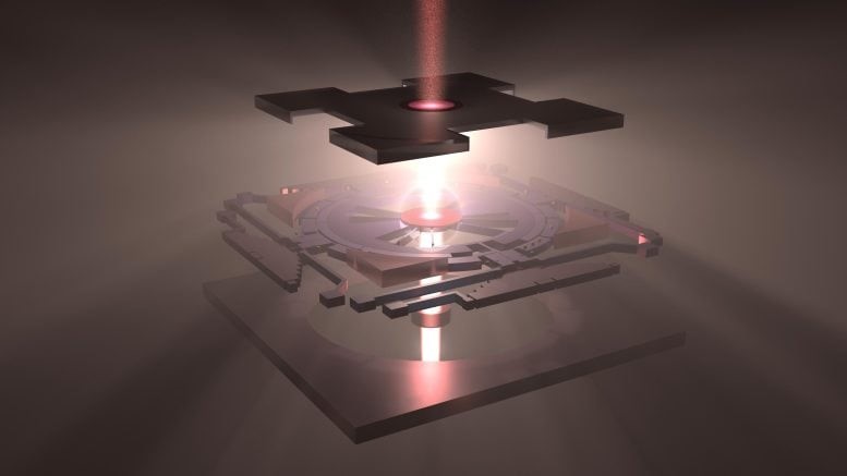
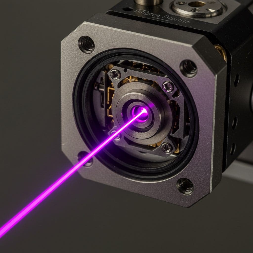
Figure 1. Revolutionizing Light with Twisted Microchips.
Despite this potential, integrating these crystals into functional devices remains a major challenge. Current systems can't actively adjust the twist or spacing in real time, significantly limiting their practical use. Figure 1 shows Revolutionizing Light with Twisted Microchips.
A Breakthrough in On-Chip Design
In an exciting development, researchers from the Harvard John A. Paulson School of Engineering and Applied Sciences (SEAS), in collaboration with Stanford University and the University of California, Berkeley, have created an on-chip twisted moiré photonic crystal sensor. This innovative sensor leverages MEMS (Micro-Electro-Mechanical Systems) technology to dynamically adjust the gap and angle between the crystal layers in real time. As a result, it can simultaneously detect and capture detailed polarization and wavelength information, marking a significant advancement in on-chip optical sensing.
Compact, Tunable, and Powerful
“Twisted moiré photonic crystals hold great promise for advancing compact and high-performance optical systems,” said Eric Mazur, the Balkanski Professor of Physics and Applied Physics at SEAS and senior author of the paper. “They offer highly tunable optical properties, precise control of light, scalable design, and wide-ranging applications across cutting-edge photonic technologies.”
“Our work shows the true potential of these materials when we can control them with precision,” added Haoning Tang, a postdoctoral fellow at SEAS and first author of the study. “It lays the groundwork for scalable, flat-optics devices capable of sophisticated light manipulation and information processing.”
Built for Scalability
The Harvard team’s device integrates layers of photonic crystals onto vertical and rotary actuators, all connected to a single electrode. Despite its powerful capabilities, the device remains just a few millimeters in size and is compatible with standard CMOS fabrication — enabling scalable, mass production using existing semiconductor foundry processes.
By precisely adjusting the spacing and rotation of the crystal layers with the actuators, the researchers achieved simultaneous hyperspectral and hyperpolarimetric imaging. This means each pixel captured by the sensor includes both rich spectral data and detailed polarization information — a first for a device with actively tunable light control.
Potential Across Industries
“These devices could be used for a range of applications including quantum computing, data communications, satellites, or medical imaging — any field where capturing clear images and detailed information about light and color is essential,” said Tang.
Looking ahead, future versions of the device could incorporate actuators with even more degrees of freedom, allowing for increasingly sophisticated control and more advanced optical functionalities.
Source: SciTECHDaily
Cite this article:
Priyadharshini S (2025), New Light Era: Twisted Crystals Power Microchip Innovation, AnaTechMaz, pp.270
Recent Post
-

Employing a Fermionic Neural Network to Determine the Ground State of Fractional Quantum Hall Liquids
When two-dimensional electron systems are exposed to magnetic fields at...
-

Million-Qubit Quantum Computer Could Break RSA-2048 in a Week, Says Google’s Craig Gidney
This paper outlines a major breakthrough in quantum computing by reducing...

Quantum Machine Learning Enhances IoT Data Prediction Using Kernel Methods
The growing volume of data from interconnected IoT devices presents new...

Quantum Optimization Set to Transform Rail Scheduling by 2028
Q-CTRL, in partnership with Network Rail and the Department for Transport...
IonQ and KISTI Partner to Boost Quantum Computing in South Korea
IonQ and the Korea Institute of Science and Technology Information (KISTI)...
-
Quantum Circuit Obfuscation Protects IP in Compilation
Researchers from the Singapore Institute of Technology developed a quantum...
-
Quantum Transduction Bridges Superconducting and Optical Systems
In their paper Quantum Transduction: Enabling Quantum Networking...
-

High-Efficiency Quantum Memory with 94.6% Fidelity and Minimal Noise
Quantum memory plays a vital role in quantum information processing by...
-
Triggered Emission Reveals New Routes for Correlated Photon Pairs
Researchers at Xi’an Jiaotong University’s Institute of Theoretical Physics...
-

Hardware-Optimized Trotterization for Heisenberg Model Quantum Simulation
The research tackles the challenge of simulating quantum dynamics using...
-

Distributed Quantum Computing Powers Scalable Algorithms and Secure Protocols
Scaling quantum computing faces major challenges in linking se parate...
-

Qiskit Integrates Machine Learning into Quantum Computing
The intersection of quantum computing and machine learning marks a major...
-

Quantum Control: Caltech Physicists Use Atomic Motion to Boost Entanglement & Computing
Researchers at Caltech, led by Professor Manuel Endres, have developed a new...
-

Quantum Communication Protocol Combines Encryption with Error Correction
Researchers have developed a unified protocol that integrates encryption...
New Light Era: Twisted Crystals Power Microchip Innovation
Twisted moiré photonic crystals operate on a simple yet powerful...