
An Interface Templated Method in Single Layer Graphene
“If graphene can be grown on an insulating substrate with a clean interface, certain devices might function better,” explained PhD student Bo Tian, who co-led the study under Xixiang Zhang’s supervision. This also opens the door to new types of graphene-based nanodevices.

Figure 1: Enhance the crystallinity of single layer graphene.
Figure 1 shows that A novel method can improve the crystallinity of large single-layer graphene, by electrically insulating its supports.
This potentially could help with the development of next-generation nanomaterial-based devices, such as very light and thin touchscreens, wearable electronic and solar cells.
The interface templated method has the potential to enhance the crystallinity of large single layer graphene sheets on insulating support.
The majority of graphene-based electronic devices require insulating supports. However, high-quality graphene films designed for industrial use are typically grown on a metal substrate, such as copper foil, before being transferred to insulating support for device fabrication.[1]
Zhang, Tian, and colleagues from Asia and Europe conducted the research, adjusted the chemical vapor deposition process, which depends on copper-catalysed methane breakdown into carbon precursors, to produce smooth single-crystal graphene monolayers on wafer-scale single-crystal substrates known as a c-plane sapphire.
The wafer-scale synthesis of adlayer-free ultra-flat single-crystal monolayer graphene on sapphire substrates. We converted polycrystalline Cu foil placed on Al2O3(0001) into single-crystal Cu (111) film. [3]
On the sapphire layer, injected active carbon atoms from the metal substrate-catalysed methane breakdown.
The carbon atoms migrated through the metallic layer toward the copper–sapphire interface, which served as a template, forming well-oriented graphene islands that eventually combined to create a sheet after multiple growth cycles. [2]
The researchers etched away any graphene that had accumulated on top of the copper film using a hydrogen–argon plasma to facilitate carbon diffusion.
They immersed the samples in liquid nitrogen before heating them rapidly to 500 oC, making the copper film easy to peel off while keeping the graphene monolayer intact. [1]
Field-effect transistors fabricated on as-grown graphene exhibited good electronic transport properties with high carrier mobilities.
This work breaks a bottleneck of synthesizing wafer-scale single-crystal monolayer graphene on insulating substrates and could contribute to next-generation graphene-based nanodevices.
References:
- https://www.innovationnewsnetwork.com/improving-crystallinity-large-single-layer-graphene/20052/
- https://www.azonano.com/news.aspx?newsID=38919
- source: https://www.nature.com/articles/s41563-021-01174-1
Cite this article:
Sri Vasagi K (2022), An interface templated method in single layer graphene, AnaTechMaz, pp. 33
Recent Post
-
Bacterio Rhodopsin Memory (BR)
Bacteriorhodopsin (BR) is one of the simplest and best studied optoelectrical transducers from the microbial (class I) opsins.....
-

Benefits of Hybridoma Technology
Hybridoma technology is a well-established method to produce monoclonal antibodies (mAbs) specific to antigens of interest...
-
An interface templated method in single layer graphene
If graphene can be grown on an insulating substrate with a clean interface, certain devices might ....
-
Bacteria-shredding insect wings inspire new antibacterial packaging
The lab-made nanotexture from an Australian-Japanese team of .....
-
Computational approach enables spatial mapping of single-cell data within tissues
A new computational approach developed by researchers .....
-

Genetic Algorithms
Genetic Algorithms(GAs) are adaptive heuristic search algorithms that belong to the larger part of evolutionary algorithms.....
-

Hidden flower petal colours ensure pollination and survival
According to scientists at Clemson University, the different invisible substances found......
-
Nanoparticle-based COVID-19 vaccine could target future infectious diseases
Just one dose of a new nanoparticle-based COVID-19 vaccine ....
-

Palm vein Authentication Technology
Palm vein authentication works by comparing the pattern of veins in the palm (which appear as blue lines)......
-
Palm vein Authentication Technology
Tiny biological computers made of DNA could revolutionize the way we diagnose and treat a slew of ......
-

Stem cell secrets allow researchers to revamp reprogramming
Researchers from the Babraham Institute's Epigenetics research program.....
-
Tiny Worms Will Help to Detect the Deadly Disease in future
Scientists recently reported that a device uses tiny worms to detect cancer.....
-
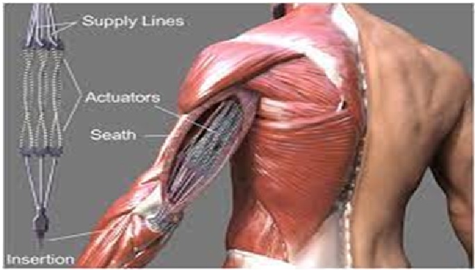
A New Nanostructured Fiber can Perform Like a Muscle Actuator
University of Texas at Austin and Penn State University Researchers, have created......
-
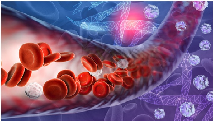
Uncovers the impact of genetic mutations on lifelong blood cell production
All human cells acquire genetic changes in their DNA throughout life,....
-

DNA Typewriter Used to Send Messages Directly into DNA
Researchers at the Howard Hughes Medical Institute (HHMI) have demonstrated....