
Breakthrough in 2D Semiconductor Technology: Scaling Up Indium Selenide for Advanced Computing
The semiconductor industry faces a significant challenge in meeting a threefold mandate: increasing computing power, decreasing chip sizes, and managing power in densely packed circuits. While silicon remains the primary material for semiconductor chips, it has limitations in terms of thickness and energy efficiency due to its three-dimensional nature. To address these challenges, researchers have been exploring two-dimensional (2D) semiconductors, which are extremely thin and offer advantages in terms of electrical control and energy efficiency.
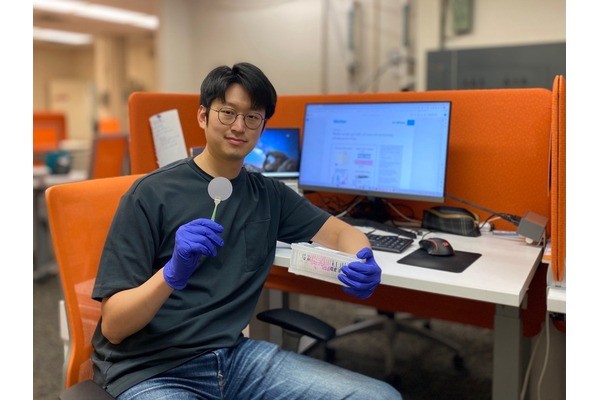
Figure 1. Seunguk Song.
Figure 1 shows postdoctoral fellow Seunguk Song. However, previous attempts to create 2D semiconductors faced various obstacles. Some materials performed well but required high temperatures for deposition, which damaged the underlying silicon chip. Others could be deposited at silicon-compatible temperatures but lacked desirable electronic properties like energy efficiency and speed. Additionally, some materials met the temperature and performance criteria but couldn't be grown to the necessary purity at standard sizes used in the industry.
Recently, a breakthrough occurred at the University of Pennsylvania School of Engineering and Applied Science, where researchers successfully grew a high-performing 2D semiconductor, indium selenide (InSe), to a full-size industrial-scale wafer. What sets InSe apart is its ability to be deposited at low temperatures, making it compatible with silicon chips.
The team, led by Associate Professor Deep Jariwala and postdoctoral fellow Seunguk Song, achieved this breakthrough by using a growth technique called "vertical metal-organic chemical vapor deposition" (MOCVD) [2]. Unlike previous methods that introduced indium and selenium simultaneously, MOCVD involved sending indium in a continuous stream while introducing selenium in pulses. This pulsing technique allowed the elements to combine in a controlled manner, maintaining a precise 50:50 ratio between them, which is crucial for the material's uniformity and performance across a full-size wafer. [1]
Furthermore, the researchers were able to control and align the direction of crystals in the material, further improving its semiconductor quality by facilitating electron transport. This development not only addressed the challenge of chemical purity but also ensured scalability, making it suitable for industrial-scale semiconductor manufacturing.
Source: University of Pennsylvania School of Engineering and Applied Science
References:
- Seunguk Song, Sungho Jeon, Mahfujur Rahaman, Jason Lynch, Dongjoon Rhee, Pawan Kumar, Srikrishna Chakravarthi, Gwangwoo Kim, Xingyu Du, Eric W. Blanton, Kim Kisslinger, Michael Snure, Nicholas R. Glavin, Eric A. Stach, Roy H. Olsson, Deep Jariwala. Wafer-scale growth of two-dimensional, phase-pure InSe. Matter, 2023; DOI: 10.1016/j.matt.2023.07.012
- University of Pennsylvania School of Engineering and Applied Science. (2023, September 19). Engineers grow full wafers of high-performing 2D semiconductor that integrates with state-of-the-art chips. ScienceDaily. Retrieved September 21, 2023 from www.sciencedaily.com/releases/2023/09/230919154851.htm
Cite this article:
Hana M (2023), Breakthrough in 2D Semiconductor Technology: Scaling Up Indium Selenide for Advanced Computing, AnaTechmaz, pp. 708