
Scientists Discover a Groundbreaking Method to Manipulate Electrons
Scientists at ETH Zurich have pioneered a novel approach to study electron interactions within materials. By utilizing a moiré material—formed by twisting ultra-thin atomic layers—they created an artificial crystal lattice in a neighboring semiconductor, enabling unprecedented precision in observing electron behavior.
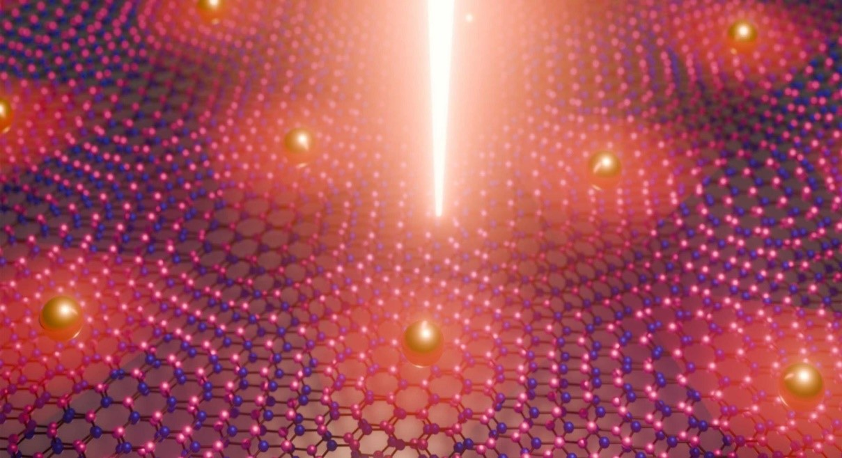
Figure 1. Two twisted boron nitride layers
Scientists have developed a technique to generate artificial crystal lattices with an expanded lattice constant in semiconductor materials. This larger lattice constant minimizes the electrons' motional energy, amplifying their interactions. The method allows researchers to explore electron behavior across various materials, potentially shedding light on how some insulators transform into superconductors when additional electrons are introduced. Figure 1 Two twisted boron nitride layers
Revealing the Secrets of Electron Interactions
Studying electron interactions, crucial for understanding phenomena like superconductivity, has long been a challenge due to their weak nature in most materials. One way to amplify these interactions is by reducing electron motional energy using artificial crystal lattices with larger lattice constants [1]. Traditionally, moiré materials—formed by stacking and slightly twisting two atom-thin layers—have been used for this purpose but often alter other material properties.
To overcome this, a team led by Ataç Imamoğlu at ETH Zurich developed a novel method using moiré materials to generate a periodic electric field that influences electrons in a separate semiconductor layer without affecting its properties. Published in Physical Review X, this approach provides a cleaner platform to study electron interactions, potentially revealing new insights into the transition of insulators to superconductors.
Twisted Crystal Lattices: Unlocking New Insights into Electron Interactions
Moiré materials are created by carefully manipulating two atom-thin layers of a material, slightly rotating one layer relative to the other, and then combining them again. This subtle misalignment causes their crystal lattices to no longer perfectly overlap, resulting in a unique "beating" effect. Similar to how two sound waves with slightly different frequencies create periodic volume fluctuations, the twisted layers generate a large-scale periodic pattern known as a "superlattice." This superlattice has a significantly larger lattice constant, allowing electrons to move within a more spacious, controlled environment.
"In our new approach, we also create a moiré material, but we utilize it in an entirely different manner," explains Natasha Kiper, a PhD student in Ataç Imamoğlu’s research group at ETH Zurich. Rather than studying the electrons within the moiré material itself, Kiper and her team use the material to generate a periodic electric field that influences electrons in an adjacent semiconductor layer.
To achieve this, the researchers stacked two layers of hexagonal boron nitride — an artificially synthesized material known for its diamond-like hardness — with a twist angle of less than 2 degrees. This subtle rotation produced a superlattice without directly altering the properties of the semiconductor, enabling the team to observe electron interactions with unprecedented clarity.
This innovative technique offers a cleaner and more controlled platform for exploring electron behavior, potentially unlocking new discoveries in quantum materials and superconductivity research.
Exciton-Based Detection of Electron Interactions
"The key advantage is that the electric field affects only the electrons in molybdenum diselenide, leaving the neutral excitons untouched," explains Kiper. Excitons, formed when electrons absorb light and leave behind positively charged holes, help researchers probe electron behavior. By analyzing the light frequency needed to excite excitons, the team could observe how electrons arranged themselves in regular patterns when one-third or two-thirds of lattice sites were filled [2]. Increasing the electron count further revealed strong interaction effects, providing insights into how certain insulators can transform into superconductors when excess electrons are introduced.
Expanding to New Materials and Phenomena
The new method offers high controllability and can be applied to various materials, says Imamoğlu. By adding more layers, the electric field strength can be adjusted, and future studies could explore electron movement between layers. This would introduce a pseudo-spin, linked to the electron's position, enabling research into exotic phenomena like chiral spin liquids, which have yet to be observed experimentally.
Reference:
- https://journals.aps.org/prx/abstract/10.1103/PhysRevX.15.011049
- https://scitechdaily.com/scientists-just-found-a-mind-bending-way-to-control-electrons/
Cite this article:
Keerthana S (2025),Scientists Discover a Groundbreaking Method to Manipulate Electrons, AnaTechmaz, pp.1105.