
Breakthrough in Solar-Blind Technology: Diamond Nanowires Establish a New Standard
Why Platinum-Embedded Diamond Nanowires Are a Game Changer
- Exceptional Responsivity: These nanowires achieve a remarkable responsivity of 68.5 A/W under 220 nm light at room temperature—about 2000 times higher than traditional oxygen-terminated bulk diamond devices. This value climbs dramatically to 3098.7 A/W at 275 °C.
- Outstanding Spectral Selectivity: They offer superior UV detection capabilities, with a UV-to-visible light rejection ratio of 550 at room temperature, which increases to an impressive 4303 at 275 °C—ideal for solar-blind applications.
- Robust Thermal and Environmental Stability: The devices maintain high performance even after 24 hours of exposure to 275 °C and remain functional after three months of atmospheric storage, proving their durability in demanding conditions.
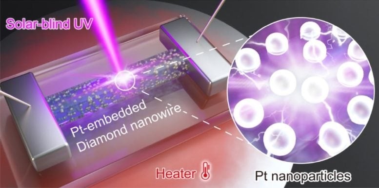
Figure 1. Revolutionizing Solar-Blind Detection: Diamond Nanowires Lead the Way.
Innovative Fabrication and Mechanisms
The platinum (Pt)-embedded diamond nanowires (DNWs) were fabricated through a novel four-step process engineered for structural precision and enhanced performance. The sequence began with the preparation of pristine DNWs, followed by the deposition of platinum films onto their surfaces. Figure 1 shows Revolutionizing Solar-Blind Detection: Diamond Nanowires Lead the Way.
These films underwent thermal dewetting to form uniformly dispersed Pt nanoparticles. Subsequently, diamond homoepitaxial growth encapsulated the nanoparticles within the nanowires. This meticulously controlled process ensures consistent nanoparticle embedding while preserving the single-crystalline structure of the DNWs.
The remarkable performance of these Pt-embedded DNWs stems from a combination of synergistic enhancement mechanisms. The one-dimensional nanowire architecture facilitates rapid, directional carrier transport, reducing scattering and improving electrical conductivity.
Concurrently, deep-level defects within the diamond lattice enhance carrier generation, broadening the photoresponse. The embedded Pt nanoparticles introduce localized surface plasmon resonance (LSPR), significantly increasing light absorption.
Additionally, localized Schottky junctions at the Pt/diamond interfaces enable efficient charge carrier separation, further improving photovoltaic and photoelectrochemical performance. Collectively, these interconnected mechanisms endow Pt-embedded DNWs with exceptional properties suited for advanced optoelectronic applications.
Future Outlook
Optimization and Application:
Ongoing research will likely focus on refining the size, distribution, and surface chemistry of Pt nanoparticles to further enhance device performance. Pt-embedded DNWs demonstrate strong potential for deployment in demanding environments—such as aerospace, industrial monitoring, and defense systems—where high-temperature resilience and reliable solar-blind UV detection are essential.
Material Exploration:
Investigating alternative metal nanoparticles or hybrid composite structures could unlock additional performance gains for diamond-based photodetectors. Furthermore, integrating these nanowires into flexible or wearable platforms may open up new avenues for next-generation optoelectronic and sensing technologies.
This research marks a significant step forward in photodetector innovation—stay tuned as the team continues to redefine the limits of high-performance, robust photodetection systems.
The Need for Solar-Blind Photodetectors
This installment introduces the concept of solar-blind photodetection—detecting ultraviolet (UV) light in the 200–280 nm range while rejecting visible and near-UV light. It explains why this selective sensitivity is vital in applications such as flame detection, space communication, industrial safety, and defense systems.
- Definition and importance of solar-blind UV detection
- Limitations of conventional materials like silicon and GaN at high temperatures or radiation-heavy environments
- Demand for materials with wide bandgaps, thermal stability, and long-term reliability
Innovation Unveiled — Platinum-Embedded Diamond Nanowires
This section delves into the breakthrough fabrication method and functional enhancements that make Pt-embedded diamond nanowires (DNWs) exceptional. It covers the four-step process (deposition, dewetting, embedding, and growth), and how these nanowires outperform traditional detectors.
- Four-step fabrication ensuring nanoparticle control and crystalline integrity
- Mechanisms enhancing performance: 1D transport, deep-level defect-induced carrier generation, LSPR, and Schottky junctions
- Performance metrics: Responsivity > 3000 A/W at elevated temperatures
- Advantages: high-temperature operation, solar-blind selectivity, mechanical robustness
A Vision Forward — Applications and Future Directions
The final part outlines potential applications and the roadmap for future research. It discusses optimizing Pt nanoparticle design, exploring new materials, and integrating DNWs into flexible, scalable platforms for widespread use.
- Application targets: aerospace, industrial safety, defense, deep-space missions
- Research frontiers: alternative nanoparticle materials, composite designs, flexible/wearable integration
- Scalability and manufacturability considerations
- Broader vision: enabling a new class of rugged, efficient photonic devices
Source:SciTECHDaily
Cite this article:
Priyadharshini S (2025), Breakthrough in Solar-Blind Technology: Diamond Nanowires Establish a New Standard, AnaTechMaz, pp.225
Recent Post
-

Physicists Unveil the First Room-Temperature 2D Altermagnet
Despite extensive theoretical and experimental research into unconventional....
-

“Zangenite” – Scientists Uncover Newly Discovered Hollow Crystal Structure
Crystals are solids formed when particles arrange themselves....
-

Cerium Shines Yellow: Chemists Discover New Behaviors in Rare Earth Elements
In rare earth elements, luminescence arises from electron transitions...
-
New Fungus-Based Material: Biodegradable, Edible and Livingn
For their research, the team selected a specific strain of the split-gill mushroom...
-

How to Overcome Bottlenecks in CO2 Capture and Conversion
Efficiently removing carbon dioxide from the atmosphere is widely.....
-

“Superwood” — 50% Stronger Than Steel — Arriving This Year
Maryland-based startup Invent Wood is gearing up to mass-produce....
-

MIT Physicists Unveil New Superconductor That Also Acts as A Magnet
Graphite consists of numerous layers of graphene—atom-thin....
-

Dry Electrode Innovation Doubles Battery Efficiency
A research team at the University of Adelaide has unveiled a breakthrough in energy...
-

Chinese Automaker-Backed Company Launches Solid-State Batteries with 136 Wh/lb Energy Density
Anhui Anwa New Energy Technology,...
-

Video: Cyborg Beetles with Backpacks May Help Locate Disaster Survivors
Researchers at the University of Queensland have transformed...
-

New Breakthrough: Scientists Transform Insulator into a Semiconductor
At the molecular level, silicones consist of a backbone of alternating....
-

Revolutionary Material Increases Solar Panel Output and Lifespan
As the global push for green energy intensifies, solar power remains a...
-

Mysterious Material Unveils Bismuth’s Quantum Secrets
Fuseya’s deep commitment to studying bismuth led him to explore phenomena....
-

A New Reign in Propylene Production: Cobalt Catalyst Surpasses Precious Metals
Chinese Academy of Sciences, in collaboration with other researchers...
-
Breakthrough in Solar-Blind Technology: Diamond Nanowires Establish a New Standard
These nanowires achieve a remarkable responsivity of 68.5 A/W under 220...